Report an Error


NVIDIA GeForce RTX 4070 AD103
- Graphics Processor
- AD103
- Cores
- 5888
- TMUs
- 184
- ROPs
- 64
- Memory Size
- 12 GB
- Memory Type
- GDDR6X
- Bus Width
- 192 bit


GPU
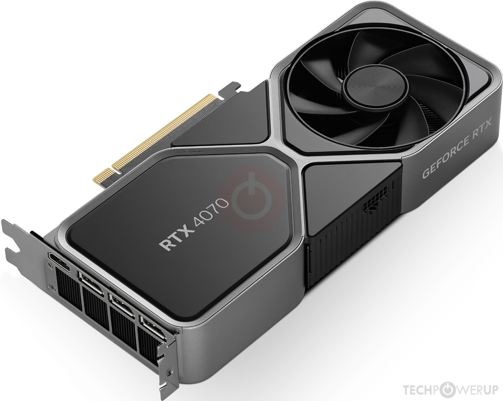
Top

Bottom

Rear

Back
Recommended Gaming Resolutions:
- 1920x1080
- 2560x1440
- 3840x2160
The GeForce RTX 4070 AD103 is a high-end graphics card by NVIDIA, launched in March 2024. Built on the 5 nm process, and based on the AD103 graphics processor, in its AD103-175-K1-A1 variant, the card supports DirectX 12 Ultimate. This ensures that all modern games will run on GeForce RTX 4070 AD103. Additionally, the DirectX 12 Ultimate capability guarantees support for hardware-raytracing, variable-rate shading and more, in upcoming video games. The AD103 graphics processor is a large chip with a die area of 379 mm² and 45,900 million transistors. Unlike the fully unlocked GeForce RTX 4080 SUPER, which uses the same GPU but has all 10240 shaders enabled, NVIDIA has disabled some shading units on the GeForce RTX 4070 AD103 to reach the product's target shader count. It features 5888 shading units, 184 texture mapping units, and 64 ROPs. Also included are 184 tensor cores which help improve the speed of machine learning applications. The card also has 46 raytracing acceleration cores. NVIDIA has paired 12 GB GDDR6X memory with the GeForce RTX 4070 AD103, which are connected using a 192-bit memory interface. The GPU is operating at a frequency of 1920 MHz, which can be boosted up to 2475 MHz, memory is running at 1313 MHz (21 Gbps effective).
Being a dual-slot card, the NVIDIA GeForce RTX 4070 AD103 draws power from 1x 16-pin power connector, with power draw rated at 200 W maximum. Display outputs include: 1x HDMI 2.1, 3x DisplayPort 1.4a. GeForce RTX 4070 AD103 is connected to the rest of the system using a PCI-Express 4.0 x16 interface. The card's dimensions are 240 mm x 110 mm x 40 mm, and it features a dual-slot cooling solution. Its price at launch was 599 US Dollars.
Being a dual-slot card, the NVIDIA GeForce RTX 4070 AD103 draws power from 1x 16-pin power connector, with power draw rated at 200 W maximum. Display outputs include: 1x HDMI 2.1, 3x DisplayPort 1.4a. GeForce RTX 4070 AD103 is connected to the rest of the system using a PCI-Express 4.0 x16 interface. The card's dimensions are 240 mm x 110 mm x 40 mm, and it features a dual-slot cooling solution. Its price at launch was 599 US Dollars.
Graphics Processor
- GPU Name
- AD103
- GPU Variant
- AD103-175-K1-A1
- Architecture
- Ada Lovelace
- Foundry
- TSMC
- Process Size
- 5 nm
- Transistors
- 45,900 million
- Density
- 121.1M / mm²
- Die Size
- 379 mm²
Graphics Card
- Release Date
- Mar 2024
- Availability
- Mar, 2024
- Generation
- GeForce 40
- Predecessor
- GeForce 30
- Production
- Active
- Launch Price
- 599 USD
- Bus Interface
- PCIe 4.0 x16
- Reviews
- 53 in our database
Relative Performance
Based on TPU review data: "Performance Summary" at 1920x1080, 4K for 2080 Ti and faster.
Performance estimated based on architecture, shader count and clocks.
Clock Speeds
- Base Clock
- 1920 MHz
- Boost Clock
- 2475 MHz
- Memory Clock
-
1313 MHz
21 Gbps effective
Memory
- Memory Size
- 12 GB
- Memory Type
- GDDR6X
- Memory Bus
- 192 bit
- Bandwidth
- 504.2 GB/s
Render Config
- Shading Units
- 5888
- TMUs
- 184
- ROPs
- 64
- SM Count
- 46
- Tensor Cores
- 184
- RT Cores
- 46
- L1 Cache
- 128 KB (per SM)
- L2 Cache
- 36 MB
Theoretical Performance
- Pixel Rate
- 158.4 GPixel/s
- Texture Rate
- 455.4 GTexel/s
- FP16 (half)
- 29.15 TFLOPS (1:1)
- FP32 (float)
- 29.15 TFLOPS
- FP64 (double)
- 455.4 GFLOPS (1:64)
Board Design
- Slot Width
- Dual-slot
- Length
- 240 mm
9.4 inches
- Width
- 110 mm
4.3 inches
- Height
- 40 mm
1.6 inches
- TDP
- 200 W
- Suggested PSU
- 550 W
- Outputs
- 1x HDMI 2.1
3x DisplayPort 1.4a
- Power Connectors
- 1x 16-pin
- Board Number
- PG141 SKU 370
Graphics Features
- DirectX
- 12 Ultimate (12_2)
- OpenGL
- 4.6
- OpenCL
- 3.0
- Vulkan
- 1.3
- CUDA
- 8.9
- Shader Model
- 6.7
AD103 GPU Notes
| Ray Tracing Cores: 3rd Gen Tensor Cores: 4th Gen NVENC: 8th Gen NVDEC: 5th Gen PureVideo HD: VP12 VDPAU: Feature Set L |
Apr 29th, 2024 14:44 EDT
change timezone
Latest GPU Drivers
New Forum Posts
- Is this Sapphire PULSE RX 5600 XT legit or fake? (14)
- Arctic MX-6 shelf life is just a couple months? (21)
- Throttlestop I7-9750H is there a risk with raising PL1 and PL2? (10)
- Is it better for zero RPM PSUs to place the fan on top? (25)
- Aorus laptop 15p kd i7 11800h rtx 3060 (1)
- i7-1355U (5)
- EK seems to be having major issues (55)
- Why MS buying all of these Studios is bad for Gaming (51)
- What's your latest tech purchase? (20392)
- Show us your collections thread!! (283)
Popular Reviews
- HYTE THICC Q60 240 mm AIO Review
- Ugreen NASync DXP4800 Plus Review
- Upcoming Hardware Launches 2023 (Updated Feb 2024)
- MOONDROP x Crinacle DUSK In-Ear Monitors Review - The Last 5%
- FiiO K19 Desktop DAC/Headphone Amplifier Review
- Thermalright Phantom Spirit 120 EVO Review
- AMD Ryzen 7 7800X3D Review - The Best Gaming CPU
- ASUS Radeon RX 7900 GRE TUF OC Review
- Logitech G Pro X Superlight 2 Review - Updated with 4000 Hz Tested
- Sapphire Radeon RX 7900 GRE Pulse Review
Controversial News Posts
- Windows 11 Now Officially Adware as Microsoft Embeds Ads in the Start Menu (148)
- Intel Statement on Stability Issues: "Motherboard Makers to Blame" (143)
- Sony PlayStation 5 Pro Specifications Confirmed, Console Arrives Before Holidays (117)
- NVIDIA Points Intel Raptor Lake CPU Users to Get Help from Intel Amid System Instability Issues (106)
- AMD "Strix Halo" Zen 5 Mobile Processor Pictured: Chiplet-based, Uses 256-bit LPDDR5X (103)
- AMD's RDNA 4 GPUs Could Stick with 18 Gbps GDDR6 Memory (101)
- US Government Wants Nuclear Plants to Offload AI Data Center Expansion (98)
- TechPowerUp Hiring: Reviewers Wanted for Motherboards, Laptops, Gaming Handhelds and Prebuilt Desktops (89)