Report an Error


NVIDIA EXK107

EXK107
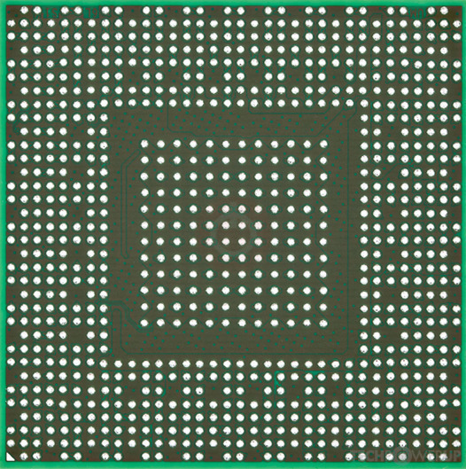
GK107 BGA
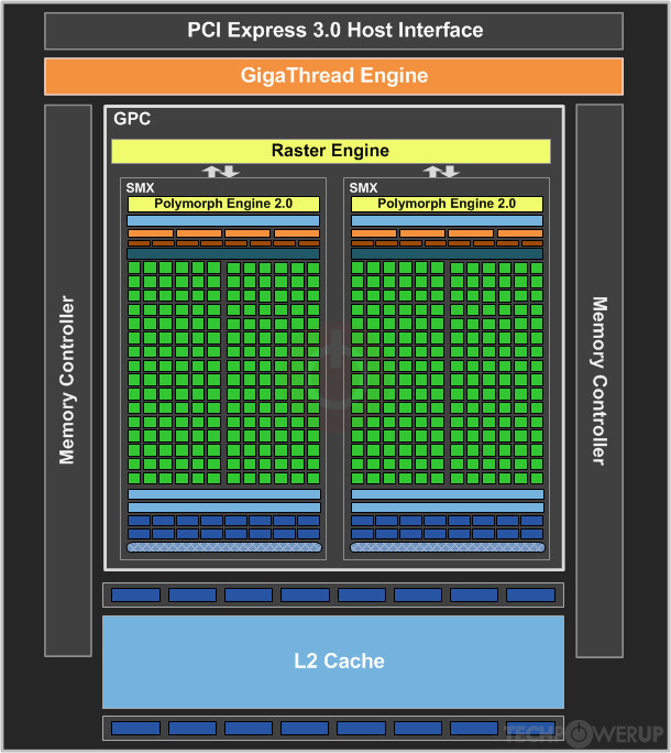
Block Diagram

SM Diagram
NVIDIA's EXK107 GPU uses the Kepler architecture and is made using a 28 nm production process at TSMC. With a die size of 118 mm² and a transistor count of 1,270 million it is a small chip. EXK107 supports DirectX 11.0 (Feature Level 11_0). For GPU compute applications, OpenCL version 3.0 and CUDA 3.0 can be used. It features 384 shading units, 32 texture mapping units and 16 ROPs.
Graphics Processor
- Released
- Mar 22nd, 2012
- GPU Name
- EXK107
- Architecture
- Kepler
- Foundry
- TSMC
- Process Size
- 28 nm
- Transistors
- 1,270 million
- Density
- 10.8M / mm²
- Die Size
- 118 mm²
- Package
- BGA-908
Graphics Features
- DirectX
- 11.0 (11_0)
- OpenGL
- 4.1
- OpenCL
- 3.0
- Vulkan
- N/A
- CUDA
- 3.0
- Shader Model
- 5.1
Render Config
- Shading Units
- 384
- TMUs
- 32
- ROPs
- 16
- SM Count
- 2
- SFUs
- 64
- GPCs
- 1
- Tex L1 Cache
- 48 KB per SMX
- L1 Cache
- 16 KB per SM
- L2 Cache
- 256 KB
- Max. TDP
- 45 W
All Kepler GPUs
NVIDIA GPU Architecture History
- 2024 Blackwell
- 2023 Hopper
- 2022-2024 Ada Lovelace
- 2020-2024 Ampere
- 2018-2022 Turing
- 2017-2020 Volta
- 2016-2021 Pascal
- 2014-2019 Maxwell 2.0
- 2014-2017 Maxwell
- 2013-2015 Kepler 2.0
- 2012-2018 Kepler
- 2010-2016 Fermi 2.0
- 2010-2013 VLIW Vec4
- 2010-2016 Fermi
- 2007-2013 Tesla 2.0
- 2006-2010 Tesla
- 2003-2013 Curie
- 2003-2005 Rankine
- 2001-2003 Kelvin
- 1999-2005 Celsius
- 1998-2000 Fahrenheit
Graphics cards using the NVIDIA EXK107 GPU
| Name | Chip | Memory | Shaders | TMUs | ROPs | Base Clock | Boost Clock | Memory Clock |
|---|---|---|---|---|---|---|---|---|
| 2 GB | 384 | 32 | 16 | 835 MHz | 1058 MHz | 900 MHz |
EXK107 GPU Notes
| L1 Cache is configurable from 16 KB up to 48 KB per SMX |
May 16th, 2024 19:06 EDT
change timezone
Latest GPU Drivers
New Forum Posts
- The Official Linux/Unix Desktop Screenshots Megathread (713)
- Ubuntu 24.04 LTS released (33)
- PC turns off unexpectedly when under (seemingly) high cpu load, but rarely (3)
- Free Games Thread (3813)
- LOL ASUS says this is $200 in repair, Steve from gamers Nexus smokes ASUS, Steam Deck til I die boys!!!! (87)
- Struck out with Asus X670E-F board, continuous 10500Hz squeal, recommend my next gamble (17)
- Hi, my GPU suddenly dropped in performance 2 days ago and i have been trying to fix it since then, my GPU clock is capped at 300 MHz (0)
- EK seems to be having major issues (83)
- HELP! VBIOS msi geforce rtx 3060 ti ventus 3x 8g oc LHR (1)
- Dell Workstation Owners Club (3093)
Popular Reviews
- Homeworld 3 Performance Benchmark Review - 35 GPUs Tested
- Enermax REVOLUTION D.F. X 1200 W Review
- Lofree Edge Ultra-Low Profile Wireless Mechanical Keyboard Review
- Silverstone Shark Force 120 mm Fan Review
- Upcoming Hardware Launches 2023 (Updated Feb 2024)
- ZMF Caldera Closed Planar Magnetic Headphones Review
- AMD Ryzen 7 7800X3D Review - The Best Gaming CPU
- Corsair MP700 Pro SE 4 TB Review
- ASUS Radeon RX 7900 GRE TUF OC Review
- Sapphire Radeon RX 7900 GRE Pulse Review
Controversial News Posts
- Intel Statement on Stability Issues: "Motherboard Makers to Blame" (267)
- AMD to Redesign Ray Tracing Hardware on RDNA 4 (227)
- Windows 11 Now Officially Adware as Microsoft Embeds Ads in the Start Menu (172)
- NVIDIA to Only Launch the Flagship GeForce RTX 5090 in 2024, Rest of the Series in 2025 (152)
- AMD Hits Highest-Ever x86 CPU Market Share in Q1 2024 Across Desktop and Server (137)
- AMD RDNA 5 a "Clean Sheet" Graphics Architecture, RDNA 4 Merely Corrects a Bug Over RDNA 3 (128)
- AMD's RDNA 4 GPUs Could Stick with 18 Gbps GDDR6 Memory (114)
- AMD Ryzen 9 7900X3D Now at a Mouth-watering $329 (104)