Report an Error


AMD Radeon 550X
- Graphics Processor
- Lexa
- Cores
- 512
- TMUs
- 32
- ROPs
- 16
- Memory Size
- 2 GB
- Memory Type
- GDDR5
- Bus Width
- 128 bit

GPU
Recommended Gaming Resolutions:
- 1600x900
- 1920x1080
- 2560x1440
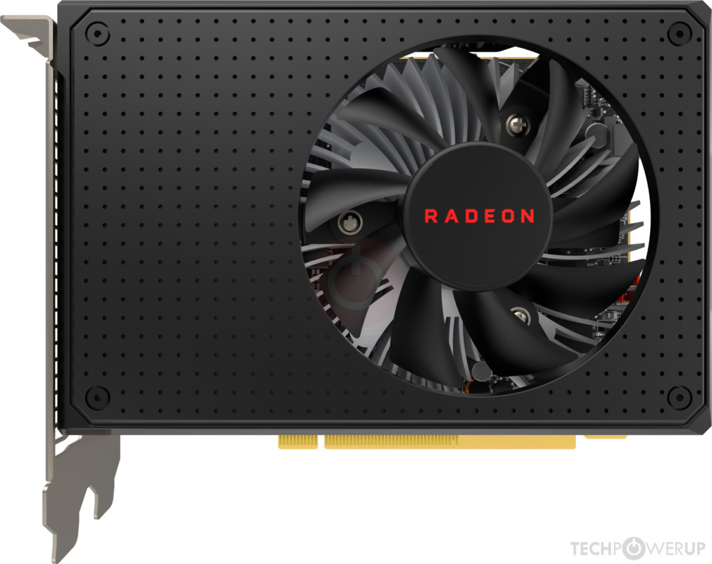
The Radeon 550X was a graphics card by AMD, launched on March 27th, 2019. Built on the 14 nm process, and based on the Lexa graphics processor, in its Lexa PRO variant, the card supports DirectX 12. This ensures that all modern games will run on Radeon 550X. The Lexa graphics processor is an average sized chip with a die area of 103 mm² and 2,200 million transistors. Unlike the fully unlocked Radeon 550X 640SP, which uses the same GPU but has all 640 shaders enabled, AMD has disabled some shading units on the Radeon 550X to reach the product's target shader count. It features 512 shading units, 32 texture mapping units, and 16 ROPs. AMD has paired 2,048 MB GDDR5 memory with the Radeon 550X, which are connected using a 128-bit memory interface. The GPU is operating at a frequency of 1082 MHz, which can be boosted up to 1218 MHz, memory is running at 1750 MHz (7 Gbps effective).
Being a dual-slot card, the AMD Radeon 550X does not require any additional power connector, its power draw is rated at 50 W maximum. Display outputs include: 1x DVI, 1x HDMI 2.0b, 1x DisplayPort 1.4a. Radeon 550X is connected to the rest of the system using a PCI-Express 3.0 x8 interface. The card measures 145 mm in length, and features a dual-slot cooling solution.
Being a dual-slot card, the AMD Radeon 550X does not require any additional power connector, its power draw is rated at 50 W maximum. Display outputs include: 1x DVI, 1x HDMI 2.0b, 1x DisplayPort 1.4a. Radeon 550X is connected to the rest of the system using a PCI-Express 3.0 x8 interface. The card measures 145 mm in length, and features a dual-slot cooling solution.
Graphics Processor
Graphics Card
Relative Performance
Based on TPU review data: "Performance Summary" at 1920x1080, 4K for 2080 Ti and faster.
Performance estimated based on architecture, shader count and clocks.
Clock Speeds
- Base Clock
- 1082 MHz
- Boost Clock
- 1218 MHz
- Memory Clock
-
1750 MHz
7 Gbps effective
Memory
- Memory Size
- 2 GB
- Memory Type
- GDDR5
- Memory Bus
- 128 bit
- Bandwidth
- 112.0 GB/s
Render Config
- Shading Units
- 512
- TMUs
- 32
- ROPs
- 16
- Compute Units
- 8
- L1 Cache
- 16 KB (per CU)
- L2 Cache
- 512 KB
Theoretical Performance
- Pixel Rate
- 19.49 GPixel/s
- Texture Rate
- 38.98 GTexel/s
- FP16 (half)
- 1,247 GFLOPS (1:1)
- FP32 (float)
- 1,247 GFLOPS
- FP64 (double)
- 77.95 GFLOPS (1:16)
Board Design
- Slot Width
- Dual-slot
- Length
- 145 mm
5.7 inches
- TDP
- 50 W
- Suggested PSU
- 250 W
- Outputs
- 1x DVI
1x HDMI 2.0b
1x DisplayPort 1.4a
- Power Connectors
- None
- Board Number
- D090
Graphics Features
- DirectX
- 12 (12_0)
- OpenGL
- 4.6
- OpenCL
- 2.1
- Vulkan
- 1.3
- Shader Model
- 6.7
Lexa GPU Notes
| Generation: Arctic Islands Codename: Polaris 12 Old Codename: Treasure Graphics/Compute: GFX8 (gfx804) Display Core Engine: 11.2 Unified Video Decoder: 6.3 Video Compression Engine: 3.4 System DMA: 3.0.0 CLRX: GCN 1.2.0 |
May 19th, 2024 09:34 EDT
change timezone
Latest GPU Drivers
New Forum Posts
- Your PC ATM (34564)
- Would you pay more for hardware with AI capabilities? (35)
- Blender 3.3.0 Benchmark (16)
- Sniper Elite 4 not syncing/capping fps below 60/90. (17)
- 7800 xt nitro+(Solved) (15)
- Cannot locate ASRock rx6800 Challenger pro OC VBIOS update (9)
- how to tell if the windows xp 64bit i bought is 64bit not 32bit (16)
- Milestones (13887)
- Horizontal black lines popping up on my screen? (16)
- WCG Daily Numbers (12520)
Popular Reviews
- Ghost of Tsushima Performance Benchmark Review - 35 GPUs Tested
- Homeworld 3 Performance Benchmark Review - 35 GPUs Tested
- Lofree Edge Ultra-Low Profile Wireless Mechanical Keyboard Review
- Silverstone Shark Force 120 mm Fan Review
- Enermax REVOLUTION D.F. X 1200 W Review
- TerraMaster D8 Hybrid Review
- Upcoming Hardware Launches 2023 (Updated Feb 2024)
- AMD Ryzen 7 7800X3D Review - The Best Gaming CPU
- AMD Radeon RX 7900 XTX Review - Disrupting the GeForce RTX 4080
- Sapphire Radeon RX 7900 GRE Pulse Review
Controversial News Posts
- Intel Statement on Stability Issues: "Motherboard Makers to Blame" (269)
- AMD to Redesign Ray Tracing Hardware on RDNA 4 (227)
- Windows 11 Now Officially Adware as Microsoft Embeds Ads in the Start Menu (173)
- NVIDIA to Only Launch the Flagship GeForce RTX 5090 in 2024, Rest of the Series in 2025 (154)
- AMD Hits Highest-Ever x86 CPU Market Share in Q1 2024 Across Desktop and Server (140)
- AMD RDNA 5 a "Clean Sheet" Graphics Architecture, RDNA 4 Merely Corrects a Bug Over RDNA 3 (135)
- AMD's RDNA 4 GPUs Could Stick with 18 Gbps GDDR6 Memory (114)
- AMD Ryzen 9 7900X3D Now at a Mouth-watering $329 (104)