Report an Error


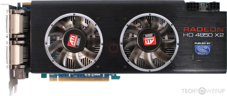
ATI Radeon HD 4850 X2
- Graphics Processor
- R700 x2
- Cores
- 800 x2
- TMUs
- 40 x2
- ROPs
- 16 x2
- Memory Size
- 512 MB x2
- Memory Type
- GDDR3
- Bus Width
- 256 bit x2

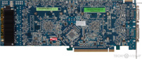
GPU
I/O

Rear

Back
Recommended Gaming Resolutions:
- 1600x900
- 1920x1080
- 2560x1440
The Radeon HD 4850 X2 was a high-end graphics card by ATI, launched on November 7th, 2008. Built on the 55 nm process, and based on the R700 graphics processor, in its R700 PRO variant, the card supports DirectX 10.1. Since Radeon HD 4850 X2 does not support DirectX 11 or DirectX 12, it might not be able to run all the latest games. The R700 graphics processor is an average sized chip with a die area of 256 mm² and 956 million transistors. Radeon HD 4850 X2 combines two graphics processors to increase performance. It features 800 shading units, 40 texture mapping units, and 16 ROPs, per GPU. ATI has paired 1,024 MB GDDR3 memory with the Radeon HD 4850 X2, which are connected using a 256-bit memory interface per GPU (each GPU manages 512 MB). The GPU is operating at a frequency of 625 MHz, memory is running at 995 MHz.
Being a dual-slot card, the ATI Radeon HD 4850 X2 draws power from 1x 6-pin + 1x 8-pin power connector, with power draw rated at 250 W maximum. Display outputs include: 4x DVI, 1x S-Video. Radeon HD 4850 X2 is connected to the rest of the system using a PCI-Express 2.0 x16 interface. The card measures 267 mm in length, and features a dual-slot cooling solution. Its price at launch was 420 US Dollars.
Being a dual-slot card, the ATI Radeon HD 4850 X2 draws power from 1x 6-pin + 1x 8-pin power connector, with power draw rated at 250 W maximum. Display outputs include: 4x DVI, 1x S-Video. Radeon HD 4850 X2 is connected to the rest of the system using a PCI-Express 2.0 x16 interface. The card measures 267 mm in length, and features a dual-slot cooling solution. Its price at launch was 420 US Dollars.
Graphics Processor
Graphics Card
- Release Date
- Nov 7th, 2008
- Generation
-
Radeon R700
(HD 4800)
- Predecessor
- Radeon R600
- Successor
- Evergreen
- Production
- End-of-life
- Launch Price
- 420 USD
- Bus Interface
- PCIe 2.0 x16
- Reviews
- 26 in our database
Relative Performance
Based on TPU review data: "Performance Summary" at 1920x1080, 4K for 2080 Ti and faster.
Performance estimated based on architecture, shader count and clocks.
Clock Speeds
- GPU Clock
- 625 MHz
- Memory Clock
-
995 MHz
1990 Mbps effective
Memory
- Memory Size
- 512 MB
- Memory Type
- GDDR3
- Memory Bus
- 256 bit
- Bandwidth
- 63.68 GB/s
Render Config
- Shading Units
- 800
- TMUs
- 40
- ROPs
- 16
- Compute Units
- 10
- L1 Cache
- 16 KB (per CU)
- L2 Cache
- 256 KB
Theoretical Performance
- Pixel Rate
- 10.00 GPixel/s
- Texture Rate
- 25.00 GTexel/s
- FP32 (float)
- 1,000 GFLOPS
- FP64 (double)
- 200.0 GFLOPS (1:5)
Board Design
- Slot Width
- Dual-slot
- Length
- 267 mm
10.5 inches
- TDP
- 250 W
- Suggested PSU
- 600 W
- Outputs
- 4x DVI
1x S-Video
- Power Connectors
- 1x 6-pin + 1x 8-pin
- Board Number
- B501
Graphics Features
- DirectX
- 10.1 (10_1)
- OpenGL
- 3.3
- OpenCL
- 1.1
- Vulkan
- N/A
- Shader Model
- 4.1
R700 GPU Notes
| Codename: Wekiva Graphics/Compute: GFX3 Display Core Engine: 3.1 Unified Video Decoder: 2.0 |
Retail boards based on this design (1)
| Name | GPU Clock | Memory Clock | Other Changes |
|---|---|---|---|
| 625 MHz | 995 MHz | 1024 MB |

Apr 29th, 2024 19:20 EDT
change timezone
Latest GPU Drivers
New Forum Posts
- Your PC ATM (34529)
- 7900 XTX Seriously lacking (17)
- Have you got pie today? (16321)
- Milestones (13875)
- WCG Daily Numbers (12501)
- TPU's Rosetta Milestones and Daily Pie Thread (1863)
- What's your latest tech purchase? (20396)
- Folding Pie and Milestones!! (9012)
- Is it better for zero RPM PSUs to place the fan on top? (30)
- Guide to proper case airflow design (30)
Popular Reviews
- Ugreen NASync DXP4800 Plus Review
- HYTE THICC Q60 240 mm AIO Review
- Upcoming Hardware Launches 2023 (Updated Feb 2024)
- MOONDROP x Crinacle DUSK In-Ear Monitors Review - The Last 5%
- Team Group T-Force Vulcan ECO DDR5-6000 32 GB CL38 Review
- Alienware Pro Wireless Gaming Keyboard Review
- AMD Ryzen 7 7800X3D Review - The Best Gaming CPU
- Thermalright Phantom Spirit 120 EVO Review
- FiiO K19 Desktop DAC/Headphone Amplifier Review
- ASUS Radeon RX 7900 GRE TUF OC Review
Controversial News Posts
- Windows 11 Now Officially Adware as Microsoft Embeds Ads in the Start Menu (152)
- Intel Statement on Stability Issues: "Motherboard Makers to Blame" (152)
- Sony PlayStation 5 Pro Specifications Confirmed, Console Arrives Before Holidays (117)
- NVIDIA Points Intel Raptor Lake CPU Users to Get Help from Intel Amid System Instability Issues (106)
- AMD's RDNA 4 GPUs Could Stick with 18 Gbps GDDR6 Memory (105)
- AMD "Strix Halo" Zen 5 Mobile Processor Pictured: Chiplet-based, Uses 256-bit LPDDR5X (103)
- US Government Wants Nuclear Plants to Offload AI Data Center Expansion (98)
- TechPowerUp Hiring: Reviewers Wanted for Motherboards, Laptops, Gaming Handhelds and Prebuilt Desktops (90)