Report an Error


AMD Radeon Pro V520
- Graphics Processor
- Navi 12
- Cores
- 2304
- TMUs
- 144
- ROPs
- 64
- Memory Size
- 8 GB
- Memory Type
- HBM2
- Bus Width
- 2048 bit

GPU
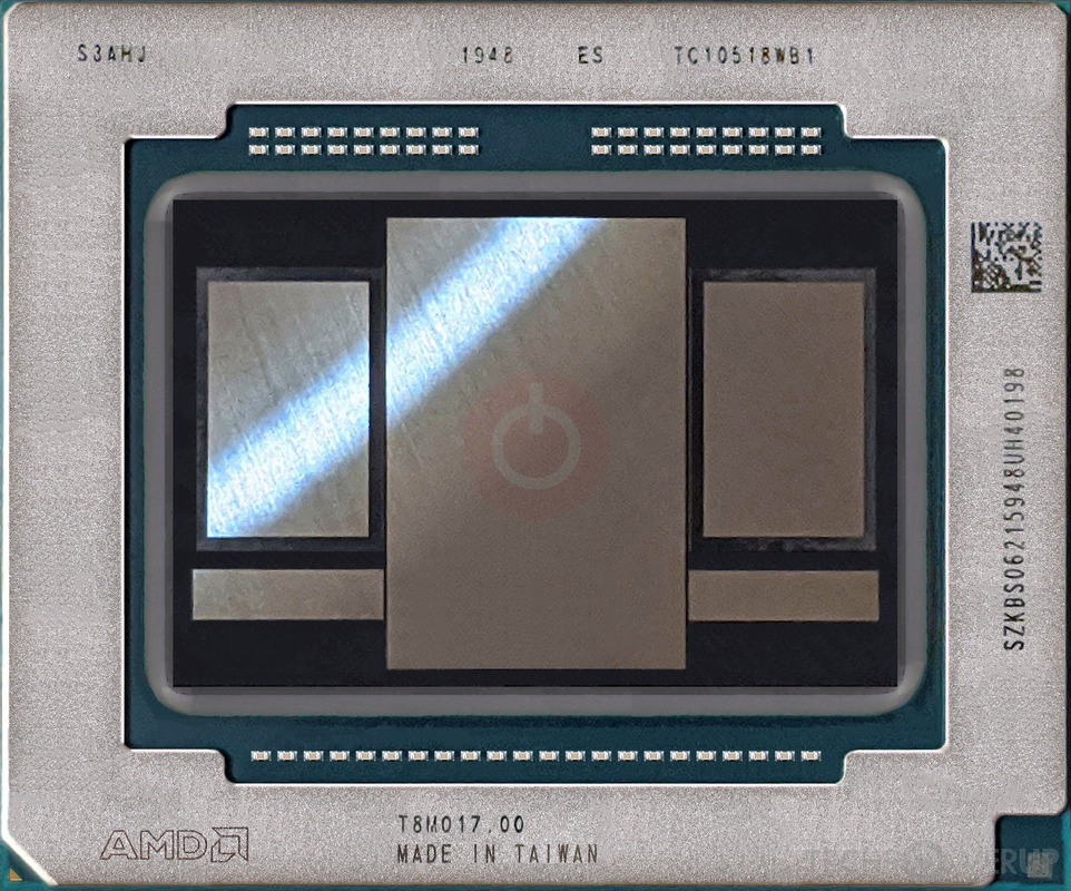
The Radeon Pro V520 is a professional graphics card by AMD, launched on December 1st, 2020. Built on the 7 nm process, and based on the Navi 12 graphics processor, in its Navi 12 GLXL variant, the card supports DirectX 12. It features 2304 shading units, 144 texture mapping units, and 64 ROPs. AMD has paired 8 GB HBM2 memory with the Radeon Pro V520, which are connected using a 2048-bit memory interface. The GPU is operating at a frequency of 1000 MHz, which can be boosted up to 1600 MHz, memory is running at 1000 MHz.
Being a dual-slot card, the AMD Radeon Pro V520 draws power from 1x 8-pin power connector, with power draw rated at 225 W maximum. This device has no display connectivity, as it is not designed to have monitors connected to it. Radeon Pro V520 is connected to the rest of the system using a PCI-Express 4.0 x16 interface. The card measures 267 mm in length, 111 mm in width, and features a dual-slot cooling solution.
Being a dual-slot card, the AMD Radeon Pro V520 draws power from 1x 8-pin power connector, with power draw rated at 225 W maximum. This device has no display connectivity, as it is not designed to have monitors connected to it. Radeon Pro V520 is connected to the rest of the system using a PCI-Express 4.0 x16 interface. The card measures 267 mm in length, 111 mm in width, and features a dual-slot cooling solution.
Graphics Processor
Graphics Card
- Release Date
- Dec 1st, 2020
- Generation
-
Radeon Pro Navi
(Navi Series)
- Predecessor
- Radeon Pro Vega
- Production
- Active
- Bus Interface
- PCIe 4.0 x16
Relative Performance
Based on TPU review data: "Performance Summary" at 1920x1080, 4K for 2080 Ti and faster.
Performance estimated based on architecture, shader count and clocks.
Clock Speeds
- Base Clock
- 1000 MHz
- Boost Clock
- 1600 MHz
- Memory Clock
-
1000 MHz
2 Gbps effective
Memory
- Memory Size
- 8 GB
- Memory Type
- HBM2
- Memory Bus
- 2048 bit
- Bandwidth
- 512.0 GB/s
Render Config
- Shading Units
- 2304
- TMUs
- 144
- ROPs
- 64
- Compute Units
- 36
- L2 Cache
- 4 MB
Theoretical Performance
- Pixel Rate
- 102.4 GPixel/s
- Texture Rate
- 230.4 GTexel/s
- FP16 (half)
- 14.75 TFLOPS (2:1)
- FP32 (float)
- 7.373 TFLOPS
- FP64 (double)
- 460.8 GFLOPS (1:16)
Board Design
- Slot Width
- Dual-slot
- Length
- 267 mm
10.5 inches
- Width
- 111 mm
4.4 inches
- TDP
- 225 W
- Suggested PSU
- 550 W
- Outputs
- No outputs
- Power Connectors
- 1x 8-pin
Graphics Features
- DirectX
- 12 (12_1)
- OpenGL
- 4.6
- OpenCL
- 2.2
- Vulkan
- 1.3
- Shader Model
- 6.7
Navi 12 GPU Notes
| Generation: Navi Graphics/Compute: 10.1.2 Shader ISA: GFX10.1 (gfx1011) Display Core Next: 2.1.0 Video Core Next: 2.0.2 System DMA: 5.0.5 Platform Security Processor: 11.0.9 CLRX: GCN 1.5.1 Per SIMD32: - 10 KB Scalar Register File Per CU: - 16 KB Vector Data Cache - 64 KB Local Data Share (GCN-Mode) Per WGP: - 16 KB Scalar Data Cache / K Cache - 32 KB Instruction Cache - 128 KB Local Data Share |
Retail boards based on this design (1)
| Name | GPU Clock | Boost Clock | Memory Clock | Other Changes |
|---|---|---|---|---|
| 1000 MHz | 1600 MHz | 1000 MHz | 150 W |

Jun 12th, 2024 03:25 EDT
change timezone
Latest GPU Drivers
New Forum Posts
- Amd confirms what I already suspected. (39)
- Current Sales, Bundles, Giveaways (10241)
- Upgrading advice on the new AMD Processors coming out.... (32)
- RX580 2048SP or RX470? Help Please (11)
- RX 580 sapphire nitro+ Problem 1340mhz + FPS + Emulator games problem (3)
- Surface Book 2 - HWMonitor not reporting CPU fan (3)
- Last game you purchased? (339)
- Good Bronze 750w PSU (6)
- What do you mostly use your desktop PC for? (Pick your top 3!) (58)
- AAF Optimus DCH Audio Modded Driver for Windows 10/11 - For ALL HDAUDIO Enumerator Chips (664)
Popular Reviews
- VAXEE Outset AX Wireless (4K) Review
- Intel Lunar Lake Technical Deep Dive - So many Revolutions in One Chip
- Upcoming Hardware Launches 2024 (Updated May 2024)
- Pulsar Xlite V3 Review
- AMD Ryzen 7 7800X3D Review - The Best Gaming CPU
- NZXT H6 Flow RGB Review
- Quick Look: Final UX2000 Wireless Noise Canceling Headphones
- Thermal Grizzly KryoSheet Review - Tested on RX 7900 XTX with 475 W
- ASUS Radeon RX 7900 GRE TUF OC Review
- Ghost of Tsushima Performance Benchmark Review - 35 GPUs Tested
Controversial News Posts
- AMD RDNA 5 a "Clean Sheet" Graphics Architecture, RDNA 4 Merely Corrects a Bug Over RDNA 3 (149)
- NVIDIA RTX 5090 "Blackwell" Founders Edition to Implement the "RTX 4090 Ti" Cinderblock Design (118)
- Possible Specs of NVIDIA GeForce "Blackwell" GPU Lineup Leaked (117)
- Nightmare Fuel for Intel: Arm CEO Predicts Arm will Take Over 50% Windows PC Market-share by 2029 (101)
- AMD Zen 5 Storms into Gaming Desktops with Ryzen 9000 "Granite Ridge" Processors (100)
- Biden Administration to Revive Trump-Era Tariffs on China-made GPUs and Motherboards (95)
- ASRock Innovates First AMD Radeon RX 7000 Graphics Card with 12V-2x6 Power Connector (94)
- AMD Ryzen 9000 Zen 5 Single Thread Performance at 5.80 GHz Found 19% Over Zen 4 (92)