Report an Error


AMD Radeon HD 7970 GHz Edition
- Graphics Processor
- Tahiti
- Cores
- 2048
- TMUs
- 128
- ROPs
- 32
- Memory Size
- 3 GB
- Memory Type
- GDDR5
- Bus Width
- 384 bit

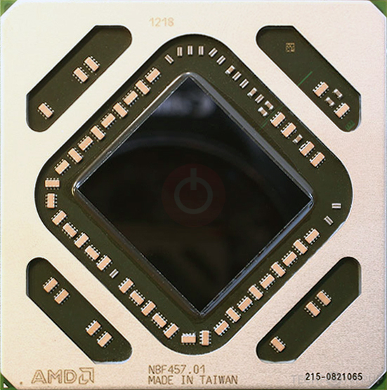
GPU
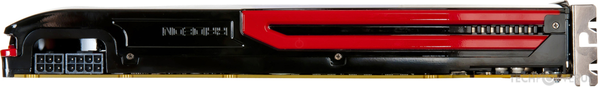
I/O
Top

Cooler
PCB Front

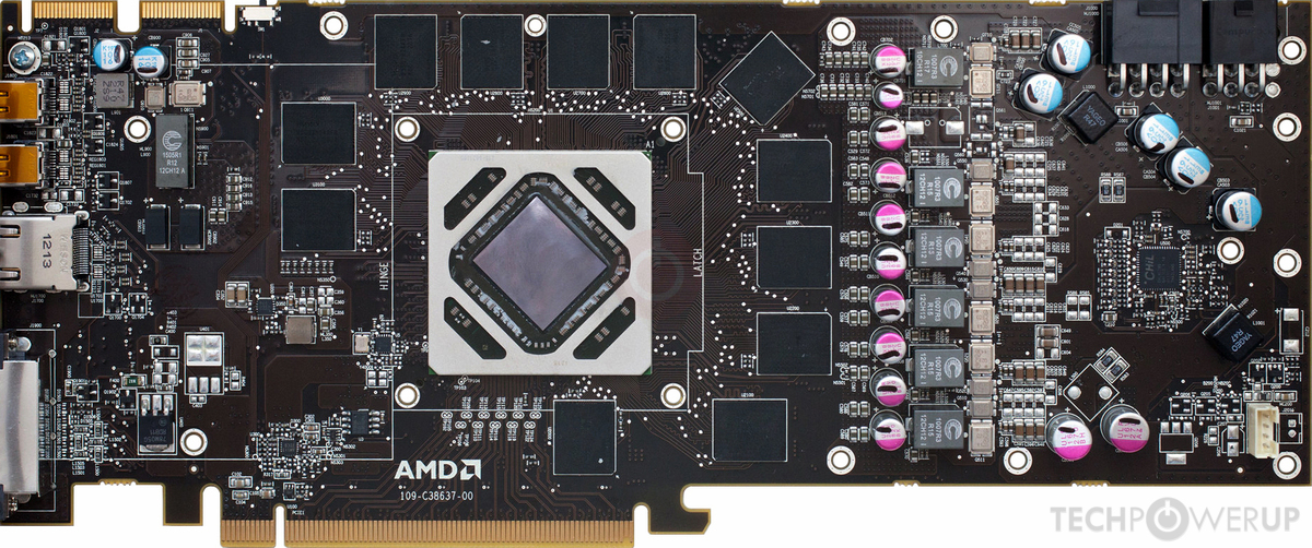
PCB Back
Recommended Gaming Resolutions:
- 1366x768
- 1600x900
- 1920x1080
The Radeon HD 7970 GHz Edition was a high-end graphics card by AMD, launched on June 22nd, 2012. Built on the 28 nm process, and based on the Tahiti graphics processor, in its Tahiti XT2 variant, the card supports DirectX 12. Even though it supports DirectX 12, the feature level is only 11_1, which can be problematic with newer DirectX 12 titles. The Tahiti graphics processor is a large chip with a die area of 352 mm² and 4,313 million transistors. It features 2048 shading units, 128 texture mapping units, and 32 ROPs. AMD has paired 3,072 MB GDDR5 memory with the Radeon HD 7970 GHz Edition, which are connected using a 384-bit memory interface. The GPU is operating at a frequency of 1000 MHz, which can be boosted up to 1050 MHz, memory is running at 1500 MHz (6 Gbps effective).
Being a dual-slot card, the AMD Radeon HD 7970 GHz Edition draws power from 1x 6-pin + 1x 8-pin power connector, with power draw rated at 300 W maximum. Display outputs include: 1x DVI, 1x HDMI 1.4a, 2x mini-DisplayPort 1.2. Radeon HD 7970 GHz Edition is connected to the rest of the system using a PCI-Express 3.0 x16 interface. The card's dimensions are 275 mm x 111 mm x 38 mm, and it features a dual-slot cooling solution. Its price at launch was 499 US Dollars.
Being a dual-slot card, the AMD Radeon HD 7970 GHz Edition draws power from 1x 6-pin + 1x 8-pin power connector, with power draw rated at 300 W maximum. Display outputs include: 1x DVI, 1x HDMI 1.4a, 2x mini-DisplayPort 1.2. Radeon HD 7970 GHz Edition is connected to the rest of the system using a PCI-Express 3.0 x16 interface. The card's dimensions are 275 mm x 111 mm x 38 mm, and it features a dual-slot cooling solution. Its price at launch was 499 US Dollars.
Graphics Processor
Graphics Card
- Release Date
- Jun 22nd, 2012
- Generation
-
Southern Islands
(HD 7900)
- Predecessor
- Northern Islands
- Successor
- Sea Islands
- Production
- End-of-life
- Launch Price
- 499 USD
- Bus Interface
- PCIe 3.0 x16
- Reviews
- 191 in our database
Relative Performance
Based on TPU review data: "Performance Summary" at 1920x1080, 4K for 2080 Ti and faster.
Clock Speeds
- Base Clock
- 1000 MHz
- Boost Clock
- 1050 MHz
- Memory Clock
-
1500 MHz
6 Gbps effective
Memory
- Memory Size
- 3 GB
- Memory Type
- GDDR5
- Memory Bus
- 384 bit
- Bandwidth
- 288.0 GB/s
Render Config
- Shading Units
- 2048
- TMUs
- 128
- ROPs
- 32
- Compute Units
- 32
- L1 Cache
- 16 KB (per CU)
- L2 Cache
- 768 KB
Theoretical Performance
- Pixel Rate
- 33.60 GPixel/s
- Texture Rate
- 134.4 GTexel/s
- FP32 (float)
- 4.301 TFLOPS
- FP64 (double)
- 1,075.2 GFLOPS (1:4)
Board Design
- Slot Width
- Dual-slot
- Length
- 275 mm
10.8 inches
- Width
- 111 mm
4.4 inches
- Height
- 38 mm
1.5 inches
- TDP
- 300 W
- Suggested PSU
- 700 W
- Outputs
- 1x DVI
1x HDMI 1.4a
2x mini-DisplayPort 1.2
- Power Connectors
- 1x 6-pin + 1x 8-pin
- Board Number
- 109-C38637-00
Graphics Features
- DirectX
- 12 (11_1)
- OpenGL
- 4.6
- OpenCL
- 2.1 (1.2)
- Vulkan
- 1.2.170
- Shader Model
- 6.5 (5.1)
Tahiti GPU Notes
| Generation: Southern Islands Desktop Variant: New Zealand / Malta Graphics/Compute: GFX6 (gfx600) Display Core Engine: 6.0 Unified Video Decoder: 3.2 Video Compression Engine: 1.0 CLRX: GCN 1.0 Exact Transistor Count: 4,312,711,873 Latest Drivers: Windows XP / 8: Catalyst Software Suite 14.4 Windows Vista : Catalyst Software Suite 13.12 Windows 7: 32-bit: Radeon Software: Adrenalin Edition 18.9.3 64-bit: AMD Software: Adrenalin Edition 22.6.1 Windows 8.1: 32-bit: Radeon Software: Crimson ReLive Edition 16.12.2 / 17.1.2 64-bit: Radeon Software: Crimson ReLive Edition 17.4.4 / 17.7.1 Windows 10: 32-bit: Radeon Software: Adrenalin Edition 18.9.3 64-bit: AMD Software: Adrenalin Edition 22.6.1 |
Retail boards based on this design (17)
| Name | GPU Clock | Boost Clock | Memory Clock | Other Changes |
|---|---|---|---|---|
| 1000 MHz | 1050 MHz | 1500 MHz | 2x DVI 1x HDMI 1x DisplayPort | |
| 1000 MHz | 1050 MHz | 1500 MHz | 279 mm/11 inches, Triple-slot, 2x DVI 4x DisplayPort | |
| 1050 MHz | 1100 MHz | 1650 MHz | 279 mm/11 inches, Triple-slot, 2x DVI 4x DisplayPort | |
| 1050 MHz | 1100 MHz | 1500 MHz | 268 mm/10.6 inches, 2x DVI 1x HDMI 2x mini-DisplayPort | |
| 1050 MHz | 1100 MHz | 1500 MHz | 268 mm/10.6 inches | |
| 1000 MHz | 1050 MHz | 1500 MHz | 2x DVI 1x HDMI 1x DisplayPort | |
| 1050 MHz | 1100 MHz | 1500 MHz | 285 mm/11.2 inches | |
| 1000 MHz | 1050 MHz | 1500 MHz | 311 mm/12.2 inches | |
| 1000 MHz | 1050 MHz | 1500 MHz | 311 mm/12.2 inches, 1x DVI 1x HDMI 4x mini-DisplayPort | |
| 1150 MHz | 1180 MHz | 1500 MHz | 311 mm/12.2 inches, 1x DVI 1x HDMI 4x mini-DisplayPort | |
| 1070 MHz | 1150 MHz | 1500 MHz | 305 mm/12 inches, 2x DVI 4x mini-DisplayPort | |
| 1020 MHz | 1100 MHz | 1500 MHz | 305 mm/12 inches, 2x DVI 4x mini-DisplayPort | |
| 1100 MHz | 1200 MHz | 1600 MHz | 6 GB, 2x DVI 1x HDMI 2x mini-DisplayPort | |
| 1000 MHz | 1050 MHz | 1500 MHz | 2x DVI 1x HDMI 1x DisplayPort | |
| 1050 MHz | 1100 MHz | 1500 MHz | 6 GB, 2x DVI 1x HDMI 2x mini-DisplayPort | |
| 1000 MHz | 1050 MHz | 1500 MHz | 268 mm/10.6 inches | |
| 1000 MHz | 1050 MHz | 1500 MHz |


Jun 27th, 2025 05:28 CDT
change timezone
Latest GPU Drivers
New Forum Posts
- What's your latest tech purchase? (24127)
- Why is the load utilization rate of my graphics card close to 100%, but the power consumption utilization rate of my graphics card is very low, far fr (11)
- Frametime spikes and stuttering after switching to AMD CPU? (452)
- PCIe5(AM5) vs PCIe4(AM4) (11)
- What are you playing? (23855)
- Anime Nation (13045)
- Hatsune Miku x ASUS TUF Gaming Build (50)
- Best time to sell your used 4090s is now. (236)
- ASUS Prime Z890 only booted the first time trying, now not even the power buttons light up. (13)
- PSU Recommendation for 3070Ti (29)
Popular Reviews
- ASRock Phantom Gaming Z890 Riptide Wi-Fi Review
- Sapphire Radeon RX 9060 XT Pulse OC 16 GB Review - Samsung Memory Tested
- SCHENKER KEY 18 Pro (E25) Review - Top-Tier Contender
- AMD Ryzen 7 9800X3D Review - The Best Gaming Processor
- Upcoming Hardware Launches 2025 (Updated May 2025)
- Lexar NQ780 4 TB Review
- Sapphire Radeon RX 9070 XT Nitro+ Review - Beating NVIDIA
- NVIDIA GeForce RTX 5060 8 GB Review
- Intel Core Ultra 7 265K Review
- AMD Ryzen 9 9950X3D Review - Great for Gaming and Productivity
TPU on YouTube
Controversial News Posts
- Intel's Core Ultra 7 265K and 265KF CPUs Dip Below $250 (280)
- NVIDIA Grabs Market Share, AMD Loses Ground, and Intel Disappears in Latest dGPU Update (203)
- Microsoft Partners with AMD for Next-gen Xbox Hardware (105)
- NVIDIA Launches GeForce RTX 5050 for Desktops and Laptops, Starts at $249 (100)
- Intel "Nova Lake‑S" Series: Seven SKUs, Up to 52 Cores and 150 W TDP (100)
- Reviewers Bemused by Restrictive Sampling of RX 9060 XT 8 GB Cards (88)
- NVIDIA GeForce RTX 5050 Reportedly Scheduled for July Release (87)
- NVIDIA GeForce RTX 5050 Uses Slower GDDR6 Memory, Based on GB207 Silicon (76)