News Posts matching #8 nm

Return to Keyword Browsing

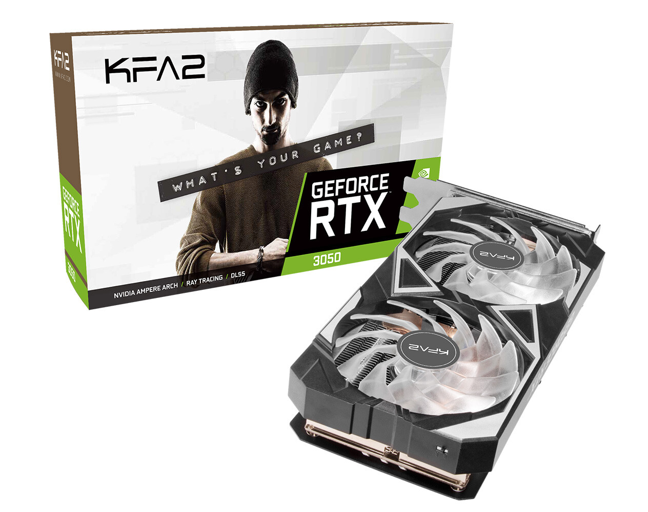
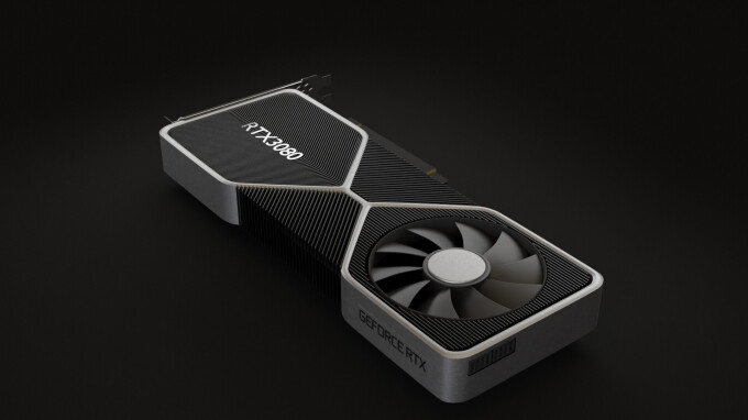
KFA2 Intros GeForce RTX 3050 6GB EX Graphics Card

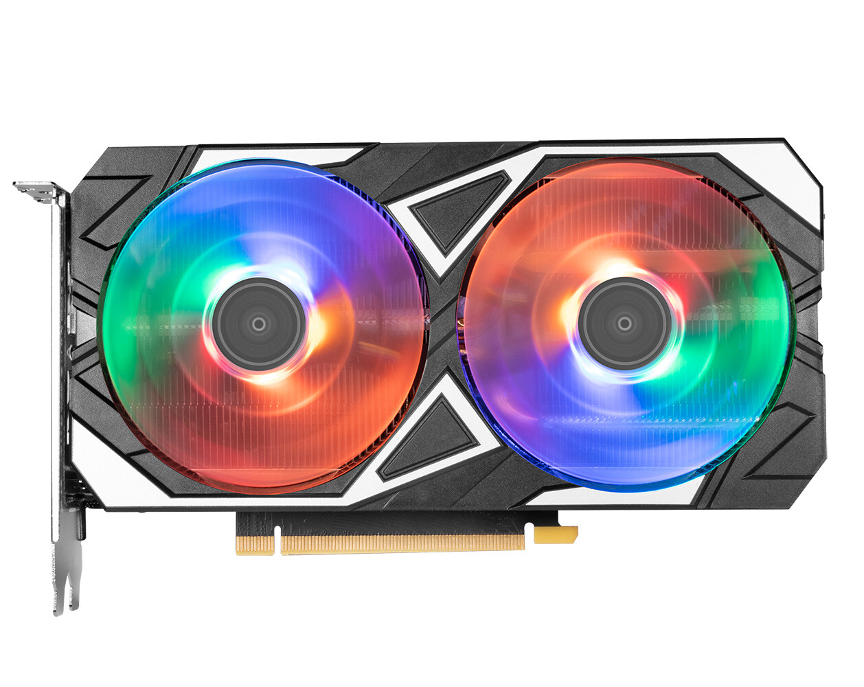
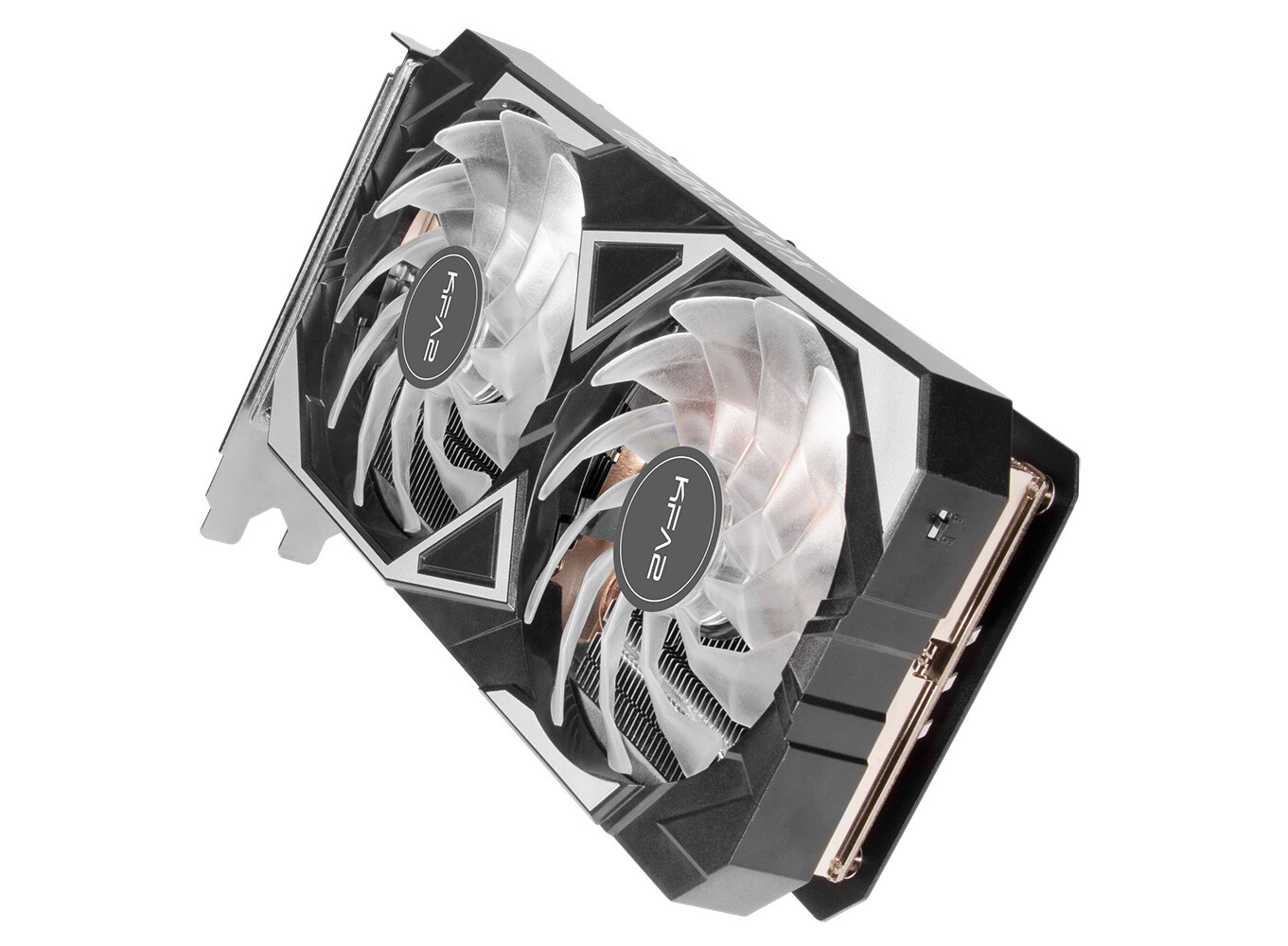
KFA2, the EU-focused brand of graphics cards by Galax, today released the GeForce RTX 3050 6 GB EX, a somewhat premium take on the recently released entry-level GPU by NVIDIA. The KFA2 EX features a spruced up aluminium fin-stack heatsink that uses a flattened copper heatpipe to make broader contact with the GPU, and spread the heat better across the fin-stack. The 22.4 cm long card also has a couple of premium touches, such as a metal backplate, and RGB LED lighting. The lighting setup includes physical switch on the tail end of the card, with which you can turn it off. Also featured is idle fan-stop. The card offers a tiny factory overclock of 1485 MHz boost, compared to 1475 MHz reference. It sticks with PCIe slot power, there are no additional power connectors.

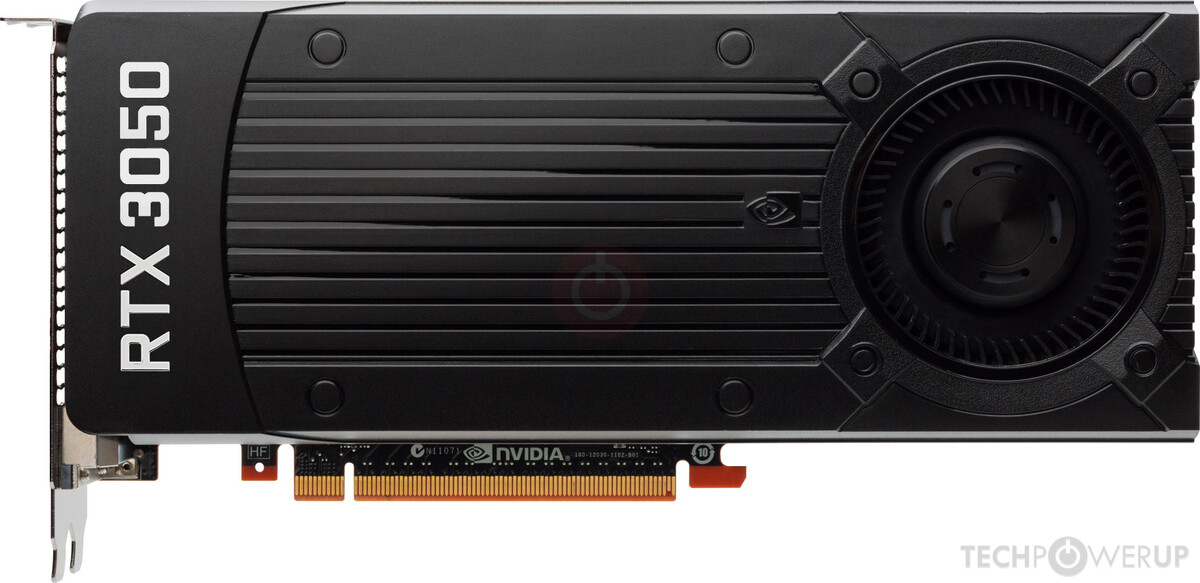
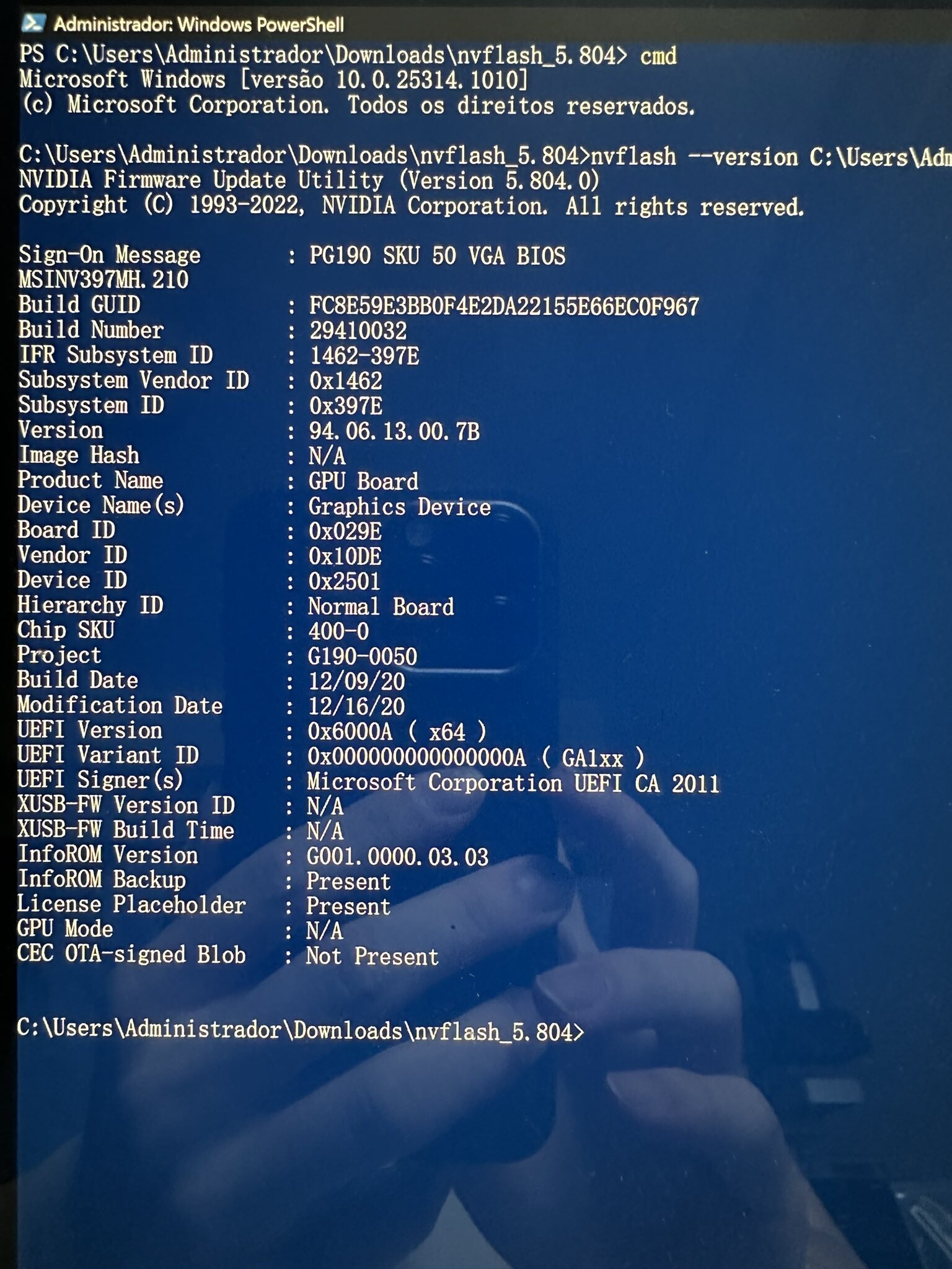
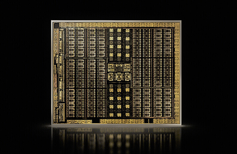
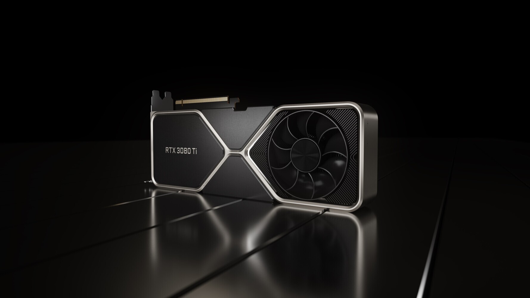
NVIDIA launched the GeForce RTX 3050 6 GB as its new entry level GPU. It is based on the older "Ampere" graphics architecture, and the 8 nm "GA107" silicon. It enables 18 out of 20 streaming multiprocessors physically present, which work out to 2,304 CUDA cores, 72 Tensor cores, 18 RT cores, 72 TMUs, and 32 ROPs. The 6 GB of 14 Gbps GDDR6 memory is spread across a narrower 96-bit memory bus than the one found in the original RTX 3050 8 GB. KFA2 is pricing the RTX 3050 6 GB EX at €199 including taxes.

ASML High-NA EUV Twinscan EXE Machines Cost $380 Million, 10-20 Units Already Booked

ASML has revealed that its cutting-edge High-NA extreme ultraviolet (EUV) chipmaking tools, called High-NA Twinscan EXE, will cost around $380 million each—over twice as much as its existing Low-NA EUV lithography systems that cost about $183 million. The company has taken 10-20 initial orders from the likes of Intel and SK Hynix and plans to manufacture 20 High-NA systems annually by 2028 to meet demand. The High-NA EUV technology represents a major breakthrough, enabling an improved 8 nm imprint resolution compared to 13 nm with current Low-NA EUV tools. This allows chipmakers to produce transistors that are nearly 1.7 times smaller, translating to a threefold increase in transistor density on chips. Attaining this level of precision is critical for manufacturing sub-3 nm chips, an industry goal for 2025-2026. It also eliminates the need for complex double patterning techniques required presently.

However, superior performance comes at a cost - literally and figuratively. The hefty $380 million price tag for each High-NA system introduces financial challenges for chipmakers. Additionally, the larger High-NA tools require completely reconfiguring chip fabrication facilities. Their halved imaging field also necessitates rethinking chip designs. As a result, adoption timelines differ across companies - Intel intends to deploy High-NA EUV at an advanced 1.8 nm (18A) node, while TSMC is taking a more conservative approach, potentially implementing it only in 2030 and not rushing the use of these lithography machines, as the company's nodes are already developing well and on time. Interestingly, the installation process of ASML's High-NA Twinscan EXE 150,000-kilogram system required 250 crates, 250 engineers, and six months to complete. So, production is as equally complex as the installation and operation of this delicate machinery.

NVIDIA GeForce RTX 3050 6GB Formally Launched

NVIDIA today formally launched the GeForce RTX 3050 6 GB as its new entry-level discrete GPU. The RTX 3050 6 GB is a significantly different product from the original RTX 3050 that the company launched as a mid-range product way back in January 2022. The RTX 3050 had originally launched on the 8 nm GA106 silicon, with 2,560 CUDA cores, 80 Tensor cores, 20 RT cores, 80 TMUs, and 32 ROPs; with 8 GB of 14 Gbps GDDR6 memory across a 128-bit memory bus; these specs also matched the maximum core-configuration of the smaller GA107 silicon, and so the company launched the RTX 3050 based on GA107 toward the end of 2022, with no change in specs, but a slight improvement in energy efficiency from the switch to the smaller silicon. The new RTX 3060 6 GB is based on the same GA107 silicon, but with significant changes.

To begin with, the most obvious change is memory. The new SKU features 6 GB of 14 Gbps GDDR6, across a narrower 96-bit memory bus, for 168 GB/s of memory bandwidth. That's not all, the GPU is significantly cut down, with just 16 SM instead of the 20 found on the original RTX 3050. This works out to 2,048 CUDA cores, 64 Tensor cores, 16 RT cores, 64 TMUs, and an unchanged 32 ROPs. The GPU comes with lower clock speeds of 1470 MHz boost, compared to 1777 MHz on the original RTX 3050. The silver lining with this SKU is its total graphics power (TGP) of just 70 W, which means that cards can completely do away with power connectors, and rely entirely on PCIe slot power. NVIDIA hasn't listed its own MSRP for this SKU, but last we heard, it was supposed to go for $179, and square off against the likes of the Intel Arc A580.

Winbond Introduces Innovative CUBE Architecture for Powerful Edge AI Devices

Winbond Electronics Corporation, a leading global supplier of semiconductor memory solutions, has unveiled a powerful enabling technology for affordable Edge AI computing in mainstream use cases. The Company's new customized ultra-bandwidth elements (CUBE) enable memory technology to be optimized for seamless performance running generative AI on hybrid edge/cloud applications.

CUBE enhances the performance of front-end 3D structures such as chip on wafer (CoW) and wafer on wafer (WoW), as well as back-end 2.5D/3D chip on Si-interposer on substrate and fan-out solutions. Designed to meet the growing demands of edge AI computing devices, it is compatible with memory density from 256 Mb to 8 Gb with a single die, and it can also be 3D stacked to enhance bandwidth while reducing data transfer power consumption.

Samsung Electronics Announces Second Quarter 2023 Results

Samsung Electronics today reported financial results for the second quarter ended June 30, 2023. The Company posted KRW 60.01 trillion in consolidated revenue, a 6% decline from the previous quarter, mainly due to a decline in smartphone shipments despite a slight recovery in revenue of the DS (Device Solutions) Division. Operating profit rose sequentially to KRW 0.67 trillion as the DS Division posted a narrower loss, while Samsung Display Corporation (SDC) and the Digital Appliances Business saw improved profitability.

The Memory Business saw results improve from the previous quarter as its focus on High Bandwidth Memory (HBM) and DDR5 products in anticipation of robust demand for AI applications led to higher-than-guided DRAM shipments. System semiconductors posted a decline in profit due to lower utilization rates on weak demand from major applications.

Unreleased GeForce RTX 3060 "Super" that Maxes Out GA106 Silicon Surfaced

An unreleased GeForce RTX 3060 "Super" graphics card surfaced on the web. The original and popular RTX 3060 falls short of maxing out the 8 nm "GA106" siicon it is based on, with 28 out of 30 streaming multiprocessors being enabled (that's 3,584 out of 3,840 CUDA cores). This odd-ball graphics card maxes the silicon out, enabling all 30 SM and 3,840 CUDA cores, 120 Tensor cores, 30 RT cores, 120 TMUs, and 48 ROPs. This card reportedly has the ASIC code "GA106-400-A1" and device ID of 10DE-2501. The memory interface is still 192-bit wide, as is the memory speed of 15 Gbps (GDDR6-effective), and it has the same 12 GB of memory. Besides more shaders, the card has been given higher clock speeds than a production RTX 3060, with up to 1875 MHz boost, compared to 1777 MHz. Alas, this is one of many unofficial rare graphics cards that never went into production, and which NVIDIA doesn't officially support with driver updates.

Strict Restrictions Imposed by US CHIPS Act Will Lower Willingness of Multinational Suppliers to Invest

TrendForce reports that the US Department of Commerce recently released details regarding its CHIPS and Science Act, which stipulates that beneficiaries of the act will be restricted in their investment activities—for more advanced and mature processes—in China, North Korea, Iran, and Russia for the next ten years. The scope of restrictions in this updated legislation will be far more extensive than the previous export ban, further reducing the willingness of multinational semiconductor companies to invest in China for the next decade.

CHIPS Act will mainly impact TSMC; and as the decoupling of the supply chain continues, VIS and PSMC capture orders rerouted from Chinese foundries
In recent years, the US has banned semiconductor exports and passed the CHIPS Act, all to ensure supply chains decoupling from China. Initially, bans on exports were primarily focused on non-planar transistor architecture (16/14 nm and more advanced processes). However, Japan and the Netherlands have also announced that they intend to join the sanctions, which means key DUV immersion systems, used for producing both sub-16 nm and 40/28 nm mature processes, are likely to be included within the scope of the ban as well. These developments, in conjunction with the CHIPS Act, mean that the expansion of both Chinese foundries and multinational foundries in China will be suppressed to varying degrees—regardless of whether they are advanced or mature processes.

Foundry Revenue is Forecasted to Drop by 4% YoY for 2023, TrendForce Notes

TrendForce's recent analysis of the foundry market reveals that demand continues to slide for all types of mature and advanced nodes. The major IC design houses have cut wafer input for 1Q23 and will likely scale back further for 2Q23. Currently, foundries are expected to maintain a lower-than-ideal level of capacity utilization rate in the first two quarters of this year. Some nodes could experience a steeper demand drop in 2Q23 as there are still no signs of a significant rebound in wafer orders. Looking ahead to the second half of this year, orders will likely pick up for some components that underwent an inventory correction at an earlier time. However, the state of the global economy will remain the largest variable that affect demand, and the recovery of individual foundries' capacity utilization rates will not occur as quickly as expected. Taking these factors into account, TrendForce currently forecasts that global foundry revenue will drop by around 4% YoY for 2023. The projected decline for 2023 is more severe when compared with the one that was recorded for 2019.

NVIDIA GeForce RTX 3060 Ti with GDDR6X to Replace Standard Model with GDDR6

NVIDIA recently updated its product stack with an 8 GB 128-bit GDDR6 variant of the GeForce RTX 3060 (originally 12 GB 192-bit GDDR6), and the RTX 3060 Ti with faster 19 Gbps 256-bit GDDR6X memory (originally 14 Gbps 256-bit GDDR6). We're getting to learn that the new RTX 3060 Ti GDDR6X variant is designed to replace the older GDDR6 variant. NVIDIA's add-in card (AIC) partners are reportedly winding down orders of the original RTX 3060 Ti in favor of the newer GDDR6X variant. Perhaps the most striking aspect of the GDDR6X variant isn't that its memory bandwidth is 35% higher than that of the original RTX 3060 Ti; but that it sells at the same price.

The new GeForce RTX 3060 Ti GDDR6X is based on the 8 nm "GA104" silicon, and has the same core-configuration as the original RTX 3060 Ti, with 4,864 CUDA cores, 152 Tensor cores, 38 RT cores, 152 TMUs, and 80 ROPs; the same GPU boost frequency of 1665 MHz, and interestingly, the same typical board power of 200 W. What's changed is the switch to 19 Gbps GDDR6X memory compared to the original's 14 Gbps GDDR6, which results in a memory bandwidth of 608 GB/s, compared to the original's 448 GB/s.

Samsung Electronics Unveils Plans for 1.4 nm Process Technology

Samsung Electronics, a world leader in advanced semiconductor technology, announced today a strengthened business strategy for its Foundry Business with the introduction of cutting-edge technologies at its annual Samsung Foundry Forum event. With significant market growth in high-performance computing (HPC), artificial intelligence (AI), 5/6G connectivity and automotive applications, demand for advanced semiconductors has increased dramatically, making innovation in semiconductor process technology critical to the business success of foundry customers. To that end, Samsung highlighted its commitment to bringing its most advanced process technology, 1.4-nanometer (nm), for mass production in 2027.

During the event, Samsung also outlined steps its Foundry Business is taking in order to meet customers' needs, including: foundry process technology innovation, process technology optimization for each specific applications, stable production capabilities, and customized services for customers. "The technology development goal down to 1.4 nm and foundry platforms specialized for each application, together with stable supply through consistent investment are all part of Samsung's strategies to secure customers' trust and support their success," said Dr. Si-young Choi, president and head of Foundry Business at Samsung Electronics. "Realizing every customer's innovations with our partners has been at the core of our foundry service."

NVIDIA AD102 "Ada" Packs Over 75 Billion Transistors

NVIDIA's next-generation AD102 "Ada" GPU is shaping up to be a monstrosity, with a rumored transistor-count north of 75 billion. This would put over 2.6 times the 28.3 billion transistors of the current-gen GA102 silicon. NVIDIA is reportedly building the AD102 on the TSMC N5 (5 nm EUV) node, which offers a significant transistor-density uplift over the Samsung 8LPP (8 nm DUV) node on which the GA102 is built. The 8LPP offers 44.56 million transistors per mm² die-area (MTr/mm²), while the N5 offers a whopping 134 MTr/mm², which fits in with the transistor-count gain. This would put its die-area in the neighborhood of 560 mm². The AD102 is expected to power high-end RTX 40-series SKUs in the RTX 4090-series and RTX 4080-series.

Top 10 Foundries Post Record 4Q21 Performance for 10th Consecutive Quarter at US$29.55B, Says TrendForce

The output value of the world's top 10 foundries in 4Q21 reached US$29.55 billion, or 8.3% growth QoQ, according to TrendForce's research. This is due to the interaction of two major factors. One is limited growth in overall production capacity. At present, the shortage of certain components for TVs and laptops has eased but there are other peripheral materials derived from mature process such as PMIC, Wi-Fi, and MCU that are still in short supply, precipitating continued fully loaded foundry capacity. Second is rising average selling price (ASP). In the fourth quarter, more expensive wafers were produced in succession led by TSMC and foundries continued to adjust their product mix to increase ASP. In terms of changes in this quarter's top 10 ranking, Nexchip overtook incumbent DB Hitek to clinch 10th place.

TrendForce believes that the output value of the world's top ten foundries will maintain a growth trend in 1Q22 but appreciation in ASP will still be the primary driver of said growth. However, since there are fewer first quarter working days in the Greater China Area due to the Lunar New Year holiday and this is the time when some foundries schedule an annual maintenance period, 1Q22 growth rate will be down slightly compared to 4Q21.

NVIDIA "Hopper" Might Have Huge 1000 mm² Die, Monolithic Design

Renowned hardware leaker kopike7kimi on Twitter revealed some purported details on NVIDIA's next-generation architecture for HPC (High Performance Computing), Hopper. According to the leaker, Hopper is still sporting a classic monolithic die design despite previous rumors, and it appears that NVIDIA's performance targets have led to the creation of a monstrous, ~1000 mm² die package for the GH100 chip, which usually maxes out the complexity and performance that can be achieved on a particular manufacturing process. This is despite the fact that Hopper is also rumored to be manufactured under TSMC's 5 nm technology, thus achieving higher transistor density and power efficiency compared to the 8 nm Samsung process that NVIDIA is currently contracting. At the very least, it means that the final die will be bigger than the already enormous 826 mm² of NVIDIA's GA100.

If this is indeed the case and NVIDIA isn't deploying a MCM (Multi-Chip Module) design on Hopper, which is designed for a market with increased profit margins, it likely means that less profitable consumer-oriented products from NVIDIA won't be featuring the technology either. MCM designs also make more sense in NVIDIA's HPC products, as they would enable higher theoretical performance when scaling - exactly what that market demands. Of course, NVIDIA could be looking to develop an MCM version of the GH100 still; but if that were to happen, the company could be looking to pair two of these chips together as another HPC product (rumored GH-102). ~2,000 mm² in a single GPU package, paired with increased density and architectural improvements might actually be what NVIDIA requires to achieve the 3x performance jump from the Ampere-based A100 the company is reportedly targeting.

NVIDIA Launches GeForce RTX 3080 12GB Graphics Card

NVIDIA today sneaked in a major update to its high-end GeForce RTX-30 "Ampere" series with the new RTX 3080 12 GB. Based on the same 8 nm "GA102" silicon as the original RTX 3080 (10 GB), the RTX 3080 Ti, the RTX 3090, and the upcoming RTX 3090 Ti, this SKU maxes out the 384-bit wide GDDR6X memory interface of the silicon, giving it 12 GB of 19.5 Gbps GDDR6X memory, resulting in a memory bandwidth of 912 GB/s, compared to 760 GB/s of the RTX 3080 (10 GB), and its 320-bit memory bus.

Memory isn't the only upgrade, the RTX 3080 12 GB gets a few more CUDA cores. With 70 out of 84 streaming multiprocessors (SM) enabled, the GPU gets 8,960 CUDA cores. In comparison, the RTX 3080 (10 GB) has 68 SM and 8,704 CUDA cores. This results in a Tensor core and TMU count of 280, and RT core count of 70. NVIDIA is positioning this SKU in between the RTX 3080 and the RTX 3080 Ti, and real-world prices of the card can be as high as $1,700, if not higher. TechPowerUp has several RTX 3080 12 GB graphics cards, but our editor and graphics card reviewer, W1zzard, is on a much-needed skiing holiday in the Alps, since we got no heads-up on this launch, and no marketing materials to help us understand the product. Hopefully NVIDIA puts out a public GeForce driver update later today, and we'll use it to test the cards we have. Expect our reviews to go live next week.

Samsung Foundry Announces GAA Ready, 3nm in 2022, 2nm in 2025, Other Speciality Nodes

Samsung Electronics, a world leader in advanced semiconductor technology, today unveiled plans for continuous process technology migration to 3- and 2-nanometer (nm) based on the company's Gate-All-Around (GAA) transistor structure at its 5th annual Samsung Foundry Forum (SFF) 2021. With a theme of "Adding One More Dimension," the multi-day virtual event is expected to draw over 2,000 global customers and partners. At this year's event, Samsung will share its vision to bolster its leadership in the rapidly evolving foundry market by taking each respective part of foundry business to the next level: process technology, manufacturing operations, and foundry services.

"We will increase our overall production capacity and lead the most advanced technologies while taking silicon scaling a step further and continuing technological innovation by application," said Dr. Siyoung Choi, President and Head of Foundry Business at Samsung Electronics. "Amid further digitalization prompted by the COVID-19 pandemic, our customers and partners will discover the limitless potential of silicon implementation for delivering the right technology at the right time."

NVIDIA Rumored to Refresh RTX 30-series with SUPER SKUs in January, RTX 40-series in Q4-2022

NVIDIA is rumored to be giving its GeForce RTX 30-series "Ampere" graphics card family a mid-term refresh by the 2022 International CES, in January; the company is also targeting Q4-2022, specifically October, to debut its next-generation RTX 40-series. The Q1 refresh will include "SUPER" branded SKUs taking over key price-points for NVIDIA, as it lands up with enough silicon that can be fully unlocked. This leak comes from Greymon55, a reliable source on NVIDIA leaks. It also aligns with the most recent pattern followed by NVIDIA to keep its GeForce product-stack updated. The company had recently released "Ti" updates to certain higher-end price-points, in response to competition from the Radeon RX 6000 "RDNA2" series.

NVIDIA's next-generation will be powered by the "Lovelace" graphics architecture that sees even more hardware acceleration for the RTX feature-set, more raytraced effects, and preparation for future APIs. It also marks NVIDIA's return to TSMC, with the architecture reportedly being designed for the 5 nm (N5) silicon fabrication node. The current-gen GeForce "Ampere" chips are being products on an 8 nm foundry node by Samsung.

NVIDIA Readying GeForce RTX 3090 SUPER, A Fully Unlocked GA102 with 400W Power?

NVIDIA is readying the GeForce RTX 3090 SUPER, the first "SUPER" series model from the RTX 30-series, following a recent round of "Ti" refreshes for its product stack. According to kopite7kimi and Greymon55, who each have a high strike-rate with NVIDIA rumors, the RTX 3090 SUPER could finally max-out the 8 nm "GA102" silicon on which nearly all high-end models from this NVIDIA GeForce generation are based. A fully unlocked GA102 comes with 10,752 CUDA cores, 336 Tensor cores, 84 RT cores, 336 TMUs, and 112 ROPs. The RTX 3090 stops short of maxing this out, with its 10,496 CUDA cores.

NVIDIA's strategy with the alleged RTX 3090 SUPER will be to not only max out the GA102 silicon, with its 10,752 CUDA cores, but also equip it with the fastest possible GDDR6X memory variant, which ticks at 21 Gbps data-rate, compared to 19.5 Gbps on the RTX 3090, and 19 Gbps on the RTX 3080 and RTX 3080 Ti. At this speed, across the chip's 384-bit wide memory bus, the RTX 3090 SUPER will enjoy 1 TB/s of memory bandwidth. Besides more CUDA cores, it's possible that the GPU Boost frequency could be increased. All this comes at a cost, though, with Greymon55 predicting a total graphics power (TGP) of at least 400 W, compared to 350 W of the RTX 3090. A product launch is expected within 2021.

NVIDIA "Ada Lovelace" Architecture Designed for N5, GeForce Returns to TSMC

NVIDIA's upcoming "Ada Lovelace" architecture, both for compute and graphics, is reportedly being designed for the 5 nanometer silicon fabrication node by TSMC. This marks NVIDIA's return to the Taiwanese foundry after its brief excursion to Samsung, with the 8 nm "Ampere" graphics architecture. "Ampere" compute dies continue to be built on TSMC 7 nm nodes. NVIDIA is looking to double the compute performance on its next-generation GPUs, with throughput approaching 70 TFLOP/s, from a numeric near-doubling in CUDA cores, generation-over-generation. These will also be run at clock speeds above 2 GHz. One can expect "Ada Lovelace" only by 2022, as TSMC N5 matures.

NVIDIA Reportedly Cutting RTX 2060 Fabrication to Focus on RTX 30-series

NVIDIA is reported to be cutting down on production of its highly popular RTX 2060 graphics card, in a bid to increase production of the RTX 30-series graphics cards that still elude most consumers looking to get one on their gaming rig. The decision may be motivated by increased margins on RTX 30-series products, as well as by the continuing component shortage in the industry, with even GDDR6 becoming a limiting factor to production capability.

While one might consider this a strange move at face value (Turing is manufactured on TSMC's 12 nm node, whilst Ampere is manufactured on Samsung's 8 nm), the fact of the matter is that there are a multitude of components required for GPUs besides the graphics processing silicon proper; and NVIDIA essentially sells ready-to-produce kits to AICs (Add-in-Card Partners) which already include all the required components, circuitry, and GPU slice to put together. And since supply on most components and even simple logic is currently strained, every component in an RTX 2060-allocated kit could be eating into final production capacity for the RTX 30-series graphics cards - hence the decision to curb the attempt to satiate pent-up demand with a last-generation graphics card and instead focusing on current-gen hardware.

NVIDIA Working on GeForce RTX 3090 Ti, ZOTAC FireStorm Changelog Confirms it

ZOTAC may have inadvertently leaked the GeForce RTX 3090 Ti. The latest version of its FireStorm utility mentions support for the RTX 3090 Ti. This would indicate that NVIDIA has been working on a new top-of-the-line graphics card that replaces the RTX 3090 as its most premium consumer graphics offering. Until now, it was expected that NVIDIA would hold onto the RTX 3090 as its top client product, with the gap between it and the RTX 3080 being filled up by the RTX 3080 Ti, to help it better compete with the AMD Radeon RX 6900 XT. AMD's introduction of the new RX 6900 XT (XTXH silicon), and more surprisingly, the introduction yielding a 10% clock-speed increase, has changed the competitive outlook of the very top of NVIDIA's product-stack.

There are no specifications out there, but in all likelihood, the GeForce RTX 3090 Ti maxes out the 8 nm "GA102" silicon. The RTX 3090 enables all but one of the 42 TPCs physically present on the silicon, and it's likely that this disabled TPC, amounting to an additional 256 CUDA cores, could be unlocked. This would put its CUDA core count at 10,752, compared to 10.496 on the RTX 3090. The only other area NVIDIA could squeeze out performance is GPU clock speeds—an approach similar to AMD's to come up with the RX 6900 XT (XTXH). The highest bins of GA102 could go into building the RTX 3090 Ti. The RTX 3090 already maxes out the 384-bit GDDR6X memory interface, uses the fastest 19.5 Gbps memory chips available, and offers a massive 24 GB of video memory, so it remains to be seen what other specs NVIDIA could tinker with to create the RTX 3090 Ti.

NVIDIA Announces GeForce RTX 3050 Ti Mobile and RTX 3050 Mobile

Alongside Intel's launch of the 11th Gen Core "Tiger Lake-H" desktop processor series, NVIDIA debuted its mid-range GeForce RTX 3050 Ti (mobile) and RTX 3050 (mobile) graphics processors. Both chips are designed with typical 3D power ranging between 35 W and 80 W. Both chips are based on the new 8 nm "GA107" silicon. This "Ampere" chip physically packs 2,560 CUDA cores across 20 streaming multiprocessors, with 80 tensor cores, 20 RT cores, and a 128-bit wide GDDR6 memory interface.

The GeForce RTX 3050 Ti (mobile) appears to be maxing out the GA107 silicon, featuring all 2,560 CUDA cores, 80 tensor cores, 20 RT cores, and 4 GB of GDDR6 memory across the chip's 128-bit wide memory bus. The RTX 3050 is slightly cut down, with 16 out of 20 SM enabled. This works out to 2,048 CUDA cores, 64 tensor cores, and 16 RT cores. The memory remains the same—4 GB GDDR6. Clock speeds will vary wildly depending on the notebook model, but typically, the RTX 3050 Ti can boost up to 1695 MHz, while the RTX 3050 can boost up to 1740 MHz. Both chips take advantage of PCI-Express 4.0 and Resizable BAR. The company didn't reveal memory clocks.

NVIDIA Earned $5 Billion During a GPU "Shortage" Quarter and Expects to Do it Again in the Next One

NVIDIA's recently published Q4-2020 + Fiscal Year 2021 results show that the alleged "GPU shortage" has had no bearing on the company's financials, with the company raking in $5 billion in revenue, in the quarter ending on January 31, 2021. In its outlook for the following quarter (Q1 FY 2022), the company expects to make another $5.30 billion (± 2%). To its credit, NVIDIA has been maintaining that the shortage of graphics cards in the retail market are a result of demand vastly outstripping supply; than a problem with the supply in and of itself (such as yields of the new 8 nm "Ampere" GPUs). The numbers show that NVIDIA's output of GPUs is fairly normal, and the problem lies with the retail supply-chain.

Crypto-currency mining and scalping are the two biggest problems affecting the availability of graphics cards in the retail market. Surging prices of crypto-currencies, coupled with the latest generation "Ampere" and RDNA2 graphics architectures having sufficient performance/Watt to mine crypto-currencies at viable scale, mean that crypto-miners are able to pick up inventory of graphics cards at wholesale; with very little making it down to retailers. Scalping is another major factor. Those with sophisticated online shopping tools are able to buy large quantities of graphics cards the moment they're available online, so they could re-sell or auction them at highly marked up prices, for profit. NVIDIA started to address the problem of miners by introducing measures that make their upcoming graphics cards artificially slower at mining, affecting the economics of using GPUs; while the problem of scalping remains at large.

AMD Reportedly in Plans to Outsource Partial Chip Production to Samsung

It's been doing the rounds in the rumor mill that AMD is looking to expand its semiconductor manufacturing partners beyond TSMC (for the 7 nm process and eventually 5 nm) and Global Foundries (12 nm process used in its I/O dies). The intention undoubtedly comes from the strain that's being placed on TSMC's production lines, as most foundry-less businesses outsource their wafer production to the Taiwanese companies' factories and manufacturing processes, which are currently the industry's best. However, as we've seen, TSMC is having a hard time scaling its production facilities to the unprecedented demand it's seeing from its consumers. The company also has recently announced it may prioritize new manufacturing capabilities for the automotive industry, which is also facing shortages in chips - and that certainly doesn't instill confidence in capacity increases for its non-automotive clients.

That's what originated form the rumor mill. Speculating, this could mean that AMD would be looking to outsource products with generally lower ASP to Samsung's foundries, instead of trying to cram even more silicon manufacturing onto TSMC's 7 nm process (where it already fabricates its Zen 3, RDNA 2, EPYC, and custom silicon solutions for latest-gen consoles). AMD might thus be planning on leveraging Samsung's 8 nm or even smaller fabrication processes as alternatives for, for example, lower-than-high-end graphics solutions and other product lines (such as APUs and FPGA production, should its acquisition of Xilinx come through).

NVIDIA, Samsung Strengthen Strategic Chip Fabrication Partnership in Deal

It seems NVIDIA and Samsung's partnership in bringing to life the green company's semiconductor designs isn't about to end anytime soon. Semiconductor analysts and insiders have said that NVIDIA and Samsung etched a new manufacturing deal on December 17th that still relates to the company's in-high-demand RTX-30 series graphics cards, which should see Samsung increase output - particularly at its Hwaseong plant - to sate the seemingly unquenchable demand from consumers and scalpers alike. The deal, which is roughly valued at "hundreds of billions won" will see Samsung double down on its 8 nm output for NVIDIA's latest gaming chips. This seems to put to rest speculation on an RTX 30-series redesign for TSMC's allegedly better 7 nm process - and according to the industry insiders, NVIDIA looked to Samsung specifically because of the need for "quick delivery of the chips".

This instills new life into Samsung's contract-based foundry business; according to market researcher TrendForce, Samsung's foundry business is expected to post a record $14.05 billion in sales this year, up 17.9% from 2019, as the company expands its client base not only through this and the previous NVIDIA deal, to Qualcomm Technologies Inc., Google, IBM, Cisco and China's Baidu. Samsung is accelerating its investment into EUV lithography in sub-7 nm processes so as to poach more customers and market share from industry behemoth and poster boy TSMC, spending 10 trillion won ($8.6 billion) to both improve technology and increase output on its foundries.

NVIDIA Announces the GeForce RTX 3060 Ti Graphics Card

NVIDIA today announced the GeForce RTX 3060 Ti, its new performance-segment graphics card that logically succeeds the GeForce RTX 2060 Super, at a starting MSRP of USD $399, with availability slated for December 2, 2020. The GPU is based on the same 8 nm "GA104" silicon as the $499 RTX 3070, but is heavily cut down, in featuring 38 out of 48 SMs (19 out of 24 TPCs), resulting in 4,864 CUDA cores, 152 Tensor cores, 38 RT cores, 152 TMUs, and 80 ROPs.

The RTX 3060 Ti is endowed with the same memory setup as the RTX 2060 Super—8 GB of 256-bit GDDR6 at 14 Gbps, yielding 448 GB/s bandwidth. NVIDIA developed a Founders Edition card based on the RTX 3060 Ti, which resembles the RTX 3070 Founders Edition with the exception of silvery metal replacing the gunmetal on the cooler frame. NVIDIA's various AIC partners have also announced their custom-design graphics cards. NVIDIA claims that the RTX 3060 Ti performs on par with the RTX 2080 Super, making it a beast for 1440p gaming with RTX-on. We put this claim to the test across our six launch-day reviews linked below.

Read the TechPowerUp reviews of NVIDIA RTX 3060 Ti Founders Edition, ASUS RTX 3060 Ti STRIX OC, Gigabyte RTX 3060 Ti Gaming OC Pro, MSI RTX 3060 Ti Gaming X Trio, Palit RTX 3060 Ti GamingPro OC, Zotac RTX 3060 Ti Twin Edge
Return to Keyword Browsing
Apr 29th, 2024 14:32 EDT change timezone

New Forum Posts

Popular Reviews

Controversial News Posts