News Posts matching #Alder Lake-S

Return to Keyword Browsing

Intel "Alder Lake" CPU Core Segmentation Sketched

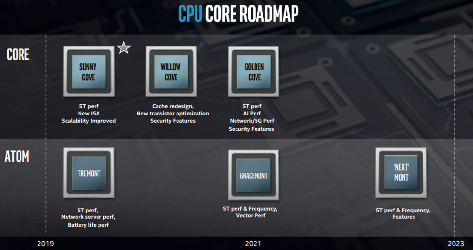
Intel's 12th Gen Core "Alder Lake-S" desktop processors in the LGA1700 package could see the desktop debut of Intel's Hybrid Technology that it introduced with the mobile segment "Lakefield" processor. Analogous to Arm big.LITTLE, Intel Hybrid Technology is a multi-core processor topology that sees the combination of high-performance CPU cores with smaller high-efficiency cores that keep the PC ticking through the vast majority of the time/tasks when the high-performance cores aren't needed and hence power-gated. The high-performance cores are woken up only as needed. "Lakefield" combines one "Sunny Cove" high-performance core with four "Tremont" low-power cores. "Alder Lake-S" will take this concept further.

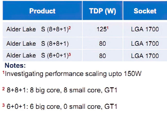
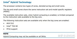
According to Intel slides leaked to the web by HXL (aka @9550pro), the 10 nm-class "Alder Lake-S" silicon will physically feature 8 "Golden Cove" high-performance cores, and 8 "Gracemont" low-power cores, along with a Gen12 iGPU that comes in three tiers - GT0 (iGPU disabled), GT1 (some execution units disabled), and GT2 (all execution units enabled). In its top trim with 125 W TDP, "Alder Lake-S" will be a "16-core" processor with 8 each of "Golden Cove" and "Gracemont" cores enabled. There will be 80 W TDP models with the same 8+8 core configuration, which are probably "locked" parts. Lastly, there the lower wrungs of the product stack will completely lack "small" cores, and be 6+0, with only high-performance cores. A recurring theme with all parts is the GT1 trim of the Gen12 iGPU.

Intel "Alder Lake-S" Confirmed to Introduce LGA1700 Socket, Technical Docs Out for Partners

Intel's Core "Alder Lake-S" desktop processor, which succeeds the 11th generation "Rocket Lake-S," is confirmed to introduce a new CPU socket, LGA1700. This new socket has been churning in the rumor mill since 2019. The LGA1700 socket is Intel's biggest mainstream desktop processor package change since LGA1156, in that the package is now physically larger, and may be cooler-incompatible with LGA115x sockets (Intel H# sockets). The enlargement in package size is seen as an attempt by Intel to give itself real-estate to build future multi-chip modules; while the increased pin-count points to the likelihood of more I/O centralization to the processor package.

The "Alder Lake-S" silicon is rumored to be Intel's first 10 nm-class mainstream desktop processor, combining a hybrid core setup of a number of "Golden Cove" high-performance CPU cores, and a number of "Gracemont" low-power cores. The processor's I/O feature-set is expected to include dual-channel DDR5 memory, PCI-Express gen 4.0, and possibly preparation for gen 5.0 on the motherboard-side. In related news, Intel put out technical documentation for the "Alder Lake-S" microarchitecture and LGA1700 socket. Access however, is restricted to Intel's industrial partners. The company also put out documentation for "Rocket Lake-S."

Intel "Sapphire Rapids," "Alder Lake" and "Tremont" Feature CLDEMOTE Instruction

Intel's three upcoming processor microarchitectures, namely the next-generation Xeon "Sapphire Rapids," Core "Alder Lake," and low-power "Tremont" cores found in Atom, Pentium Silver, Celeron, and even Core Hybrid processors, will feature a new instruction set that aims to speed up processor cache performance, called CLDEMOTE "cache line demote." This is a means for the operating system to tell a processor core that a specific content of a cache (a cache line), isn't needed to loiter around in a lower cache level (closer to the core), and can be demoted to a higher cache level (away from the core); though not flushed back to the main memory.

There are a handful benefits to what CLDEMOTE does. Firstly, it frees up lower cache levels such as L1 and L2, which are smaller in size and dedicated to a CPU core, by pushing cache lines to the last-level cache (usually L3). Secondly, it enables rapid load movements between cores by pushing cache lines to L3, which is shared between multiple cores; so it could be picked up by a neighboring core. Dr. John McCalpin from UT Austin wrote a detailed article on CLDEMOTE.

Intel "Alder Lake" LGA1700 to Feature DDR5; "Rocket Lake" Thermal Specs Leaked

PTT leaked some juicy details of the upcoming Intel "Rocket Lake" and "Alder Lake" processor generations. "Rocket Lake" will power Intel's 11th generation Core processor series in the LGA1200 package, and are rumored to be a "back port" of Intel's advanced "Willow Cove" CPU cores to a 14 nm-class silicon fabrication node, with core-counts ranging up to 8. The idea for Intel is to sell high IPC, high clock-speed desktop processors for gaming.

According to the PTT report, there will be three kinds of SKUs for "Rocket Lake" based on TDP: 8-core parts with 95 W TDP rating; and 8-core, 6-core, and 4-core parts in 80 W TDP and 65 W TDP variants. For the 95 W (PL1) parts, the power-levels PL2, and PL4 are reportedly set at 173 W and 251 W, respectively, and a 56-second Tau (a timing variable that dictates how long a processor can stick around at an elevated power-state before retreating to PL1, which is interchangeable with the TDP value on the box). The 80 W TDP parts feature 146 W PL2, 191 W PL3, and 251 W PL4, but a lower Tau value of 28 seconds. For the 65 W parts, the PL2 is 128 W, PL3 is 177 W, and PL4 251 W, and the Tau value 28 seconds.

Intel's next LGA1700 Socket to Last Over Two Generations

The upcoming LGA1700 socket by Intel, which makes its debut with 12th generation Core "Alder Lake-S" desktop processors, could be the first in over a decade from the company, to support more than two processor generations. Intel has maintained streak of ensuring that a mainstream desktop CPU socket won't be compatible with more than two generations of Core processors. Controversy brew when the company artificially segmented the LGA1151 socket between the 6th, 7th, and 8th and 9th processor generations, with the latter two requiring a 300-series chipset motherboard and the former two not working on the newer chipset, even though all four generations are pin-compatible, and modders have been able to get the newer chips to work on older 100-series and 200-series motherboards with great success.

According to a NotebookCheck report, Intel is designing the LGA1700 socket to support at least three future generations of Core processors (that's "Alder Lake-S" and two of its successors). This should give the platform a degree of longevity as it introduces several new computing concepts to the client desktop form-factor, such as heterogenous CPU cores. "Alder Lake-S" combines 8 each of low-power "Gracemont" and high performance "Golden Cove" CPU cores in a setup rivaling the Arm big.LITTLE, where light computing workloads and system idling are completely handled by the low-power cores, while the high-performance cores are only woken up from their power-gated slumber as needed, before being put back to sleep when they're not.

Rumor: Intel to Introduce Big.Little Architecture for Desktop With Alder Lake-S, New LGA 1700 Socket

Hold on to your helmets: a wild rumor that Intel may be looking to introduce the same design considerations as they already did with their Lakefield architecture has appeared. According to momomo via Twitter (a user who has already shared many rumors and details in the PC hardware space) as well as some other sources, Intel is looking to bring a Big.Little-like design (which Intel calls Hybrid architecture) to the desktop platform in the form of Alder Lake-S, to be reportedly built on the 10 nm process. While Intel's Lakefield (especially geared for the mobile market) only sported four Atom (Intel's low power) Tremont cores combined with one high-performance Sunny Cove core, Alder Lake-S could sport as many as an 8+8 configuration, with a TDP currently set up to 80 W (and up to 125 W TDP is also set in the revealing slides with a disclosure regarding investigating performance scaling in up to 150 W TDP).

Should this actual Alder Lake-S product materialize in the 10 nm process, this could be a way for Intel to salvage what it can from the 10 nm process for the desktop platform. As we know from multiple reports on the state of Intel's 10 nm, yields and operating frequencies aren't close to what was expected, and Intel's CFO George Davis even said at last week's Morgan Stanley's Analyst Conference that their 10 nm process wouldn't be as profitable as even 22 nm, which does show that Intel is already looking past this process for their 7 nm deployment. A Big.Little design for a desktop architecture does seem like a more plausible design decision for a struggling process than a full 16-core monolithic die such as those Intel currently employs.
Intel Alder Lake S Lineup Intel CPU Roadmap
Return to Keyword Browsing
Jun 11th, 2024 18:26 EDT change timezone

New Forum Posts

Popular Reviews

Controversial News Posts