Monday, July 13th 2020

Intel "Alder Lake" CPU Core Segmentation Sketched
Intel's 12th Gen Core "Alder Lake-S" desktop processors in the LGA1700 package could see the desktop debut of Intel's Hybrid Technology that it introduced with the mobile segment "Lakefield" processor. Analogous to Arm big.LITTLE, Intel Hybrid Technology is a multi-core processor topology that sees the combination of high-performance CPU cores with smaller high-efficiency cores that keep the PC ticking through the vast majority of the time/tasks when the high-performance cores aren't needed and hence power-gated. The high-performance cores are woken up only as needed. "Lakefield" combines one "Sunny Cove" high-performance core with four "Tremont" low-power cores. "Alder Lake-S" will take this concept further.
According to Intel slides leaked to the web by HXL (aka @9550pro), the 10 nm-class "Alder Lake-S" silicon will physically feature 8 "Golden Cove" high-performance cores, and 8 "Gracemont" low-power cores, along with a Gen12 iGPU that comes in three tiers - GT0 (iGPU disabled), GT1 (some execution units disabled), and GT2 (all execution units enabled). In its top trim with 125 W TDP, "Alder Lake-S" will be a "16-core" processor with 8 each of "Golden Cove" and "Gracemont" cores enabled. There will be 80 W TDP models with the same 8+8 core configuration, which are probably "locked" parts. Lastly, there the lower wrungs of the product stack will completely lack "small" cores, and be 6+0, with only high-performance cores. A recurring theme with all parts is the GT1 trim of the Gen12 iGPU.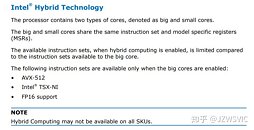 Intel is innovating a way to reconcile the vast feature-set and ISA differences between its "big" and "small" cores. The big "Golden Cove" core supports certain AVX-512 instructions, besides TSX-NI (tensor operations, matrix multiplication), and FP16 (half precision floating point). The smaller "Gracemont" core lacks these instruction sets. So whenever the OS sends traffic that requires these instructions, the processor will be forced to wake up a "Golden Cove" core, and additional such cores as needed.
A quick reminder of the LGA1700 socket - this platform could see Intel introducing PCI-Express 5.0 I/O. There's also a possibility of DDR5 unbuffered memory support. The significant increase in pin-count for the mainstream-desktop segment is probably attributable to a Ryzen-like nucleation of platform I/O over from the PCH to the CPU socket, along with more CPU-attached PCIe lanes.
Sources:
HXL (Twitter), VideoCardz, Zhihu (Forums)
According to Intel slides leaked to the web by HXL (aka @9550pro), the 10 nm-class "Alder Lake-S" silicon will physically feature 8 "Golden Cove" high-performance cores, and 8 "Gracemont" low-power cores, along with a Gen12 iGPU that comes in three tiers - GT0 (iGPU disabled), GT1 (some execution units disabled), and GT2 (all execution units enabled). In its top trim with 125 W TDP, "Alder Lake-S" will be a "16-core" processor with 8 each of "Golden Cove" and "Gracemont" cores enabled. There will be 80 W TDP models with the same 8+8 core configuration, which are probably "locked" parts. Lastly, there the lower wrungs of the product stack will completely lack "small" cores, and be 6+0, with only high-performance cores. A recurring theme with all parts is the GT1 trim of the Gen12 iGPU.

A quick reminder of the LGA1700 socket - this platform could see Intel introducing PCI-Express 5.0 I/O. There's also a possibility of DDR5 unbuffered memory support. The significant increase in pin-count for the mainstream-desktop segment is probably attributable to a Ryzen-like nucleation of platform I/O over from the PCH to the CPU socket, along with more CPU-attached PCIe lanes.
16 Comments on Intel "Alder Lake" CPU Core Segmentation Sketched
(1) Another layer of software optimization required for switching between high and low performance cores, which may cause issues due to buggy driver/ OS
(2) Consumer are forced to pay Intel extra for the Tremont cores that they don't needI was thinking the same thing as well. Just so that they can advertise as having "up to 16 cores".
I know that there's "vzeroupper", which helps differentiate between SSE and AVX code. If a 256-bit register is "half full" of zeros and flagged by vzeroupper, then Windows knows to only save 128-bits instead of 256-bits between context switches. (community.intel.com/t5/Intel-ISA-Extensions/What-is-the-status-of-VZEROUPPER-use/td-p/1098375).
I'd imagine that a similar flag is used for AVX512. Saving 1/2 or 1/4th the registers is certainly a noble goal and probably already implemented in Linux and Windows. I'm not expert enough to know if that's the case for sure... but that'd be my guess for what Intel is going for here.
This doesn't have any damned benefit in the Desktop LGA processors, even in the Alienware Area51M series or Clevo P870DM series LGA notebooks nobody gives a fuck about the damn big little like phones, where the li-ion battery power sipping increases rapidly by the higher performance cores in the ARM SoC along with ton of other dedicated modules for RF/GPU/Memory etc. Maybe their Mobile might benefit but still at the loss of powerful cores it's a hogwash, when AMD's BGA processors are beating Intel BGA lineup at perf/efficiency, loss - loss unless the ST performance of 8 physical cores is higher along with those 8 or 4 HT cores (RKL has 4 cores HT disabled as per rumors) .
This requires a lot of OS work AGAIN, AMD's NUMA processors had already seen their lack of adoption even AMD abandoned them, X399 didn't have support for the TR3000, and afaik only Milan moved more parts to the powerful cloud service providers like AWS. So Apple also probably thought along with their R&D cash into A series ARM processors a huge waste of money to put into OS rewrite when their Mac sales are also just 10% of their profit cut better spend it on their own x86-ARM translation and A series SoC since many users are into ultra thin and light and don't care about BGA BS or not.
This doesn't paint a good picture as Intel doesn't have any confidence in their lineup also this looks like a temporary band aid again on the LGA1700. I hope AMD doesn't chase this bullshit and stay true to their Desktop performance x86 leadership. TBH This won't make to Xeon for sure, having a cheap arse crappy cores on the Xeon means server OS / Software / HW changes NO ONE wants to do that. Esp when Ryzen is piledriving and steamrolling with their EPYC and RYZEN CPUs on both Server and Consumer DIY.
Netflix still uses Zen2 in its NUMA mode for far faster performance. See this for details: people.freebsd.org/~gallatin/talks/euro2019.pdf
Many programmers are unaware of the benefits of NUMA. So what Zen2 proves is that your UMA-mode needs to be reasonably fast, but not necessarily as fast as your NUMA mode. For the few programmers willing to go the extra mile and NUMA-optimize their code, NUMA will likely remain the fastest way of doing things as chiplets continue to become more common.
----------
Intel also does SubNumaClustering (SNC) for a similar effect on Skylake / Cascade Lake systems. When you have 16, 32, 64 cores... it turns out that some RAM locations are "closer" than others depending on the core you're using. The reality of NUMA is inevitable as we get more and more cores.
The question is if UMA-emulation (by round-robin distributing the data across all memory controllers) will remain fast enough that we can ignore the difficulties of NUMA in typical workloads. (IE: Zen2). But NUMA is the underlying ground truth of the physics and reality of these chips.
Tremont cores were about 1/4 the area of Sunny Cove cores on Lakefield, based on die pictures I've seen posted.