News Posts matching #Foundry

Return to Keyword Browsing

This Week in Gaming (Week 18)

As we go from April to May, we have something of a void of new game releases, with the biggest release being a game that puts you in charge of a factory. As for the rest of this coming week's releases, you can look forward to doing some farming, working as a detective, cosplaying as an alien, working in a lab and finishing the week in office with a party royale.

Foundry / This week's major release / Thursday 2 May / Early Access
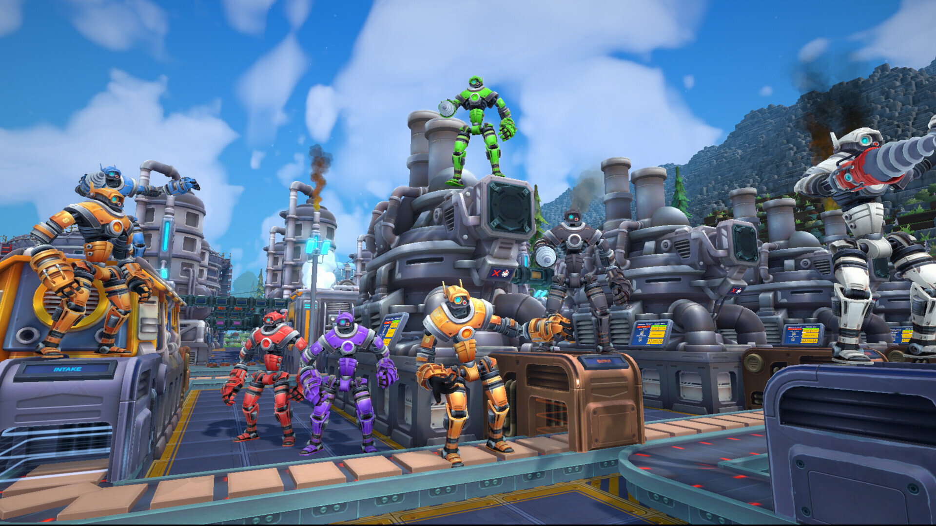
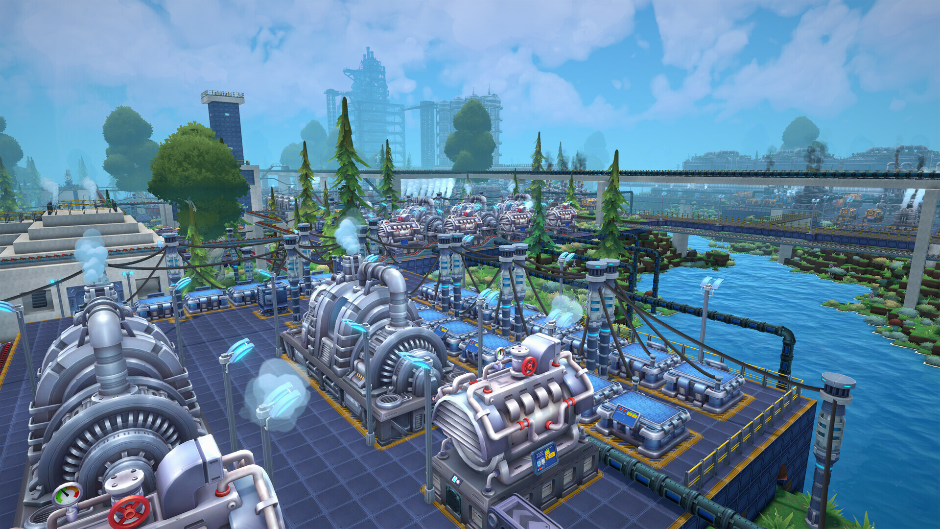
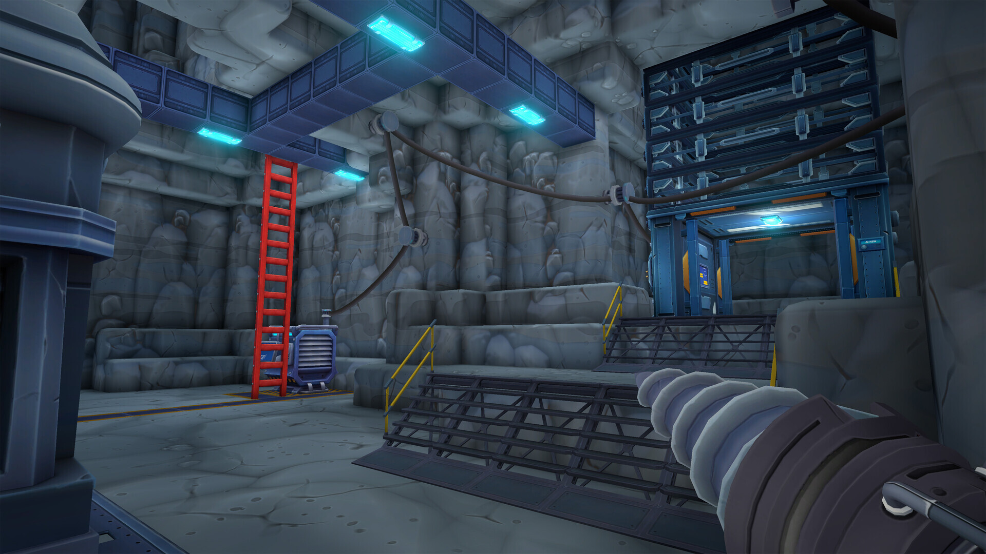
Foundry is a first-person (first-robot?) factory builder with complete creative freedom set in a procedurally generated and infinite voxel world. Land on an unexplored planet and design a giant automated robot production facility under the watchful direction of your AI friend, Carl. Steam Link

Intel Outlines New Financial Reporting Structure

Intel Corporation today outlined a new financial reporting structure that is aligned with the company's previously announced foundry operating model for 2024 and beyond. This new structure is designed to drive increased cost discipline and higher returns by providing greater transparency, accountability and incentives across the business. To support the new structure, Intel provided recast operating segment financial results for the years 2023, 2022 and 2021. The company also shared a targeted path toward long-term growth and profitability of Intel Foundry, as well as clear goals for driving financial performance improvement and shareholder value creation.

"Intel's differentiated position as both a world-class semiconductor manufacturer and a fabless technology leader creates significant opportunities to drive long-term sustainable growth across these two complementary businesses," said Pat Gelsinger, Intel CEO. "Implementing this new model marks a key achievement in our IDM 2.0 transformation as we hone our execution engine, stand up the industry's first and only systems foundry with geographically diverse leading-edge manufacturing capacity, and advance our mission to bring AI Everywhere."

Intel Redefines the Foundry for an Era of AI

Artificial intelligence isn't just driving headlines and stock valuations. It's also "pushing the boundaries of silicon technology, packaging technology, the construction of silicon, and the construction of racks and data centers," says Intel's Bob Brennan. "There is an insatiable demand," Brennan adds. Which is great timing since his job is to help satisfy that demand.

Brennan leads customer solutions engineering for Intel Foundry, which aims to make it as easy and fast as possible for the world's fabless chipmakers to fabricate and assemble their chips through Intel factories. "We are engaged from architecture to high-volume manufacturing—soup to nuts—and we present the customer with a complete solution," Brennan asserts.

US Government to Announce Massive Grant for Intel's Arizona Facility

According to the latest report by Reuters, the US government is preparing to announce a multi-billion dollar grant for Intel's chip manufacturing operations in Arizona next week, possibly worth more than $10 billion. US President Joe Biden and Commerce Secretary Gina Raimondo will make the announcement, which is part of the 2022 CHIPS and Science Act aimed at expanding US chip production and reducing dependence on China and Taiwan manufacturing. The exact amount of the grant has yet to be confirmed, but rumors suggest it could exceed $10 billion, making it the most significant award yet under the CHIPS Act. The funding will include grants and loans to bolster Intel's competitive position and support the company's US semiconductor manufacturing expansion plans. This comes as a surprise just a day after the Pentagon reportedly refused to invest $2.5 billion in Intel as a part of a secret defense grant.

Intel has been investing significantly in its US expansion, recently opening a $3.5 billion advanced packaging facility in New Mexico, supposed to create extravagant packaging technology like Foveros and EMIB. The chipmaker is also expanding its semiconductor manufacturing capacity in Arizona, with plans to build new fabs in the state. Arizona is quickly becoming a significant hub for semiconductor manufacturing in the United States. In addition to Intel's expansion, Taiwan Semiconductor Manufacturing Company (TSMC) is also building new fabs in the state, attracting supply partners to the region. CHIPS Act has a total funding capacity of $39 billion allocated for semiconductor production and $11 billion for research and development. The Intel grant will likely cover the production part, as Team Blue has been reshaping its business units with the Intel Product and Intel Foundry segments.

TSMC Aiming to Recruit Approximately 6000 New Workers

Taiwan's Commercial Times has published coverage of a newly launched TSMC recruitment drive—proceedings kicked off last weekend with company representatives heading to the National Taiwan University campus. On the second of March, TSMC set up an outdoor booth on the grounds of Taipei's public research university—where the national comprehensive institute organized a Talent Recruitment Enterprise Expo. Unsurprisingly, TSMC recruiters are seeking potential "talents with high enthusiasm for semiconductors." Ctee's reporter found out that Taiwan's premier foundry is expecting to: "recruit approximately 6,000 new colleagues in Taiwan in 2024, including engineers and technicians." TSMC is reportedly responding to business growth and technology development demands—so much so, that its native manufacturing plants require a fresh influx of workers.

According to Ctee's report, TSMC's March recruitment tour is due to snake through Taiwan and then head over to mainland China: "Tsinghua University, National Cheng Kung University, National Yang-Ming Jiaotong University, Central China University, Zhongxing University, Zhongshan, National Chung Cheng University, Beijing University of Science and Technology, etc., totaling 19 physical activities and four online talent recruitment briefings." A parallel "2024 DNA Summer Internship Program" has also been rolled out: "inviting interested students to join and use internships to personally experience the environment and culture of TSMC." The company's growing global layout also provides opportunities for new employees to work overseas—the article highlights TSMC's newly opened semiconductor fabrication plant in Kumamoto Prefecture, Japan as the preferred choice for "internal employees." The multinational firm's Arizona facilities did not get a shout out, despite recent good news. Reports from mid-2023 suggest that TSMC's core values are at odds with North American work culture.

Samsung Foundry Renames 3 nm Process to 2 nm Amid Competition with Intel

In a move that could intensify competition with Intel in the cutting-edge chip manufacturing space, Samsung Foundry has reportedly decided to rebrand its second-generation 3 nm-class fabrication technology, previously known as SF3, to a 2 nm-class manufacturing process called SF2. According to reports from ZDNet, the renaming of Samsung's SF3 to SF2 is likely an attempt by the South Korean tech giant to simplify its process nomenclature and better compete against Intel Foundry, at least visually. Intel is set to roll out its Intel 20A production node, a 2 nm-class technology, later this year. The reports suggest that Samsung has already notified its customers about the changes in its roadmap and the renaming of SF3 to SF2. Significantly, the company has reportedly gone as far as re-signing contracts with customers initially intended to use the SF3 production node.

"We were informed by Samsung Electronics that the 2nd generation 3 nm [name] is being changed to 2 nm," an unnamed source noted to ZDNet. "We had contracted Samsung Foundry for the 2nd generation 3 nm production last year, but we recently revised the contract to change the name to 2 nm." Despite the name change, Samsung's SF3, now called SF2, has not undergone any actual process technology alterations. This suggests that the renaming is primarily a marketing move, as using a different process technology would require customers to rework their chip designs entirely. Samsung intends to start manufacturing chips based on the newly named SF2 process in the second half of 2024. The SF2 technology, which employs gate-all-around (GAA) transistors that Samsung brands as Multi-Bridge-Channel Field Effect Transistors (MBCFET), does not feature a backside power delivery network (BSPDN), a significant advantage of Intel's 20A process. Samsung Foundry has not officially confirmed the renaming.

Samsung Foundry Reportedly Producing 2 nm Prototypes for Qualcomm

Smartphone chipset industry watchdogs believe that the Samsung 3 nm GAA process did not meet customer expectations, due to alleged yield issues. TSMC is seemingly victorious in this segment, as reports suggest that a next-generation 3 nm node production goal of "100,000 monthly wafers by the end of 2024" has been set. Three days ago, Samsung Foundry revealed that it is working on a very advanced SF2 GAAFET process—press outlets in South Korea propose that the manufacturing giant is hoping to outmuscle its main rival in a future 2 nm node category. Tuesday's press introduction stated that a development partnership is set: "to deliver optimized next generation ARM Cortex -X CPU developed on Samsung Foundry's latest Gate-All-Around (GAA) process technology."

A Sedaily article posits that the company's cutting-edge manufacturing tech has already attracted interest from notable parties: "Samsung Electronics is taking advantage of these advantages to win orders for the 2 nm project. Samsung Electronics took its first step by winning an order to produce a 2 nm AI accelerator from Preferred Networks (PFN), Japan's largest AI company. Qualcomm, the world's largest system semiconductor design company, has entered into discussions with Samsung Electronics' System LSI Division, which designs high-performance chips, to produce 2 nm prototypes." December 2023 news reports suggested that Samsung leadership was considering a 2 nm wafer price discount—in order to stay competitive with competing foundry services. It is possible that Qualcomm is evaluating the 2 nm SF2 GAAFET process for a distant Snapdragon 8 "Gen 5" chipset, while Samsung LSI could be working on a 2 nm "Exynos 2600" SoC design.

Intel Foundry Services (IFS) and Cadence Design Systems Expand Partnership on SoC Design

Intel Foundry Services (IFS) and Cadence Design Systems Inc. today announced a multiyear strategic agreement to jointly develop a portfolio of key customized intellectual property (IP), optimized design flows and techniques for Intel 18A process technology featuring RibbonFET gate-all-around transistors and PowerVia backside power delivery. Joint customers of the companies will be able to accelerate system-on-chip (SoC) project schedules on process nodes from Intel 18A and beyond while optimizing for performance, power, area, bandwidth and latency for demanding artificial intelligence, high performance computing and premium mobile applications.

"We're very excited to expand our partnership with Cadence to grow the IP ecosystem for IFS and provide choice for customers," said Stuart Paann, Intel senior vice president and general manager of IFS. "We will leverage Cadence's world-class portfolio of leading IP and advanced design solutions to enable our customers to deliver high-volume, high-performance and power-efficient SoCs on Intel's leading-edge process technologies."

SMIC Concerned About Financial Performance in 2024

Semiconductor Manufacturing International Corporation (SMIC) posted better than expected fourth quarter 2023 financial tallies, but issued a warning with a downward revisement of near future gross margin expectations. According to DigiTimes Asia and TrendForce, China's leading pure-play semiconductor foundry has experienced an overall decline in net profit due to various cited factors including: "the industry downturn, weak market demand, high industry inventory, and fierce competition among peers, all contributing to reduced capacity utilization and decreased wafer shipment for the group." The DigiTimes report focuses mainly on a significant SMIC shares plunge—stock prices are reported to have dropped by ~20% in early 2024, indicating a loss of confidence in the foundry's prospects.

TrendForce laid out the financial nitty gritty: "SMIC International saw a revenue increase of over 3.5% to more than USD 1.678 billion, marking the only quarter of revenue growth last year. Net profit plummeted by 54.7% to nearly USD 175 million. The gross margin of 16.4% was almost halved compared to the same period in 2022 and experienced a significant decline from the previous three quarters, reaching its lowest point of the year. In the full year of 2023, SMIC International experienced a revenue decline of over 13% to USD 6.3 billion, with a net profit decrease of 50.4% to USD 900 million. The gross margin was approximately halved to 19.3%." Many industry watchdogs believed that SMIC was in a comfortable position, thanks to an uptick in demand for natively developed AI GPUs—their flagship Shanghai plants are reportedly churning out 7 nm wafers for Huawei's Ascend 910B model. Insiders also claim that high profile smartphone clients are pushing for 5 nm production lines—a significant challenge for the foundry's existing collection of (less than cutting-edge) equipment.

TSMC Overtakes Intel and Samsung to Become World's Largest Semiconductor Maker by Revenue

Taiwan Semiconductor Manufacturing Company (TSMC) has reached a significant milestone, overtaking Intel and Samsung to become the world's largest semiconductor maker by revenue. According to Taiwanese financial analyst Dan Nystedt, TSMC earned $69.3 billion in revenue in 2023, surpassing Intel's $63 billion and Samsung's $58 billion. This is a remarkable achievement for the Taiwanese chipmaker, which has historically lagged behind Intel and Samsung in terms of revenue despite being the world's largest semiconductor foundry. TSMC's meteoric rise has been fueled by the increased demand for everything digital - from PCs to game consoles - during the coronavirus pandemic in 2020, and AI demand in the previous year. With its cutting-edge production capabilities allowing it to manufacture chips using the latest process technologies, TSMC has pulled far ahead of Intel and Samsung and can now charge a premium for its services.

This is reflected in its financials. For the 6th straight quarter, TSMC's Q4 2023 revenue of $19.55 billion also beat Intel's $15.41 billion and Samsung's $16.42 billion chip division revenue. As the world continues its rapid transformation in the AI era of devices, TSMC looks set to hold on to its top position for the foreseeable future. Its revenue and profits will likely continue to eclipse those of historical giants like Intel and Samsung. However, a big contender is Intel Foundry Services, which is slowly starting to gain external customers. If IFS takes off and new customers start adopting Intel as their foundry of choice, team blue could regain leadership in the coming years.

Intel Foundry Services Get 18A Order: Arm-based 64-Core Neoverse SoC

Faraday Technology Corporation, a Taiwanese silicon IP designer, has announced plans to develop a new 64-core system-on-chip (SoC) utilizing Intel's most advanced 18A process technology. The Arm-based SoC will integrate Arm Neoverse compute subsystems (CSS) to deliver high performance and efficiency for data centers, infrastructure edge, and 5G networks. This collaboration brings together Faraday, Arm, and Intel Foundry Services. Faraday will leverage its ASIC design and IP solutions expertise to build the SoC. Arm will provide the Neoverse compute subsystem IP to enable scalable computing. Intel Foundry Services will manufacture the chip using its cutting-edge 18A process, which delivers one of the best-in-class transistor performance.

The new 64-core SoC will be a key component of Faraday's upcoming SoC evaluation platform. This platform aims to accelerate customer development of data center servers, high-performance computing ASICs, and custom SoCs. The platform will also incorporate interface IPs from the Arm Total Design ecosystem for complete implementation and verification. Both Arm and Intel Foundry Services expressed excitement about working with Faraday on this advanced Arm-based custom silicon project. "We're thrilled to see industry leaders like Faraday and Intel on the cutting edge of Arm-based custom silicon development," said an Arm spokesperson. Intel SVP Stuart Pann said, "We are pleased to work with Faraday in the development of the SoC based on Arm Neoverse CSS utilizing our most competitive Intel 18A process technology." The collaboration represents Faraday's strategic focus on leading-edge technologies to meet evolving application requirements. With its extensive silicon IP portfolio and design capabilities, Faraday wants to deliver innovative solutions and break into next-generation computing design.

Intel Reportedly Selects TSMC's 2 Nanometer Process for "Nova Lake" CPU Generation

A Taiwan Economic Daily news article proposes that a couple of high profile clients are considering TSMC's 2 nanometer process—Apple is widely believed to be the first customer to join the foundry's queue for cutting edge services. The report posits that Intel is also signed up on the Taiwanese firm's 2 nm reservation list—TSMC is expected to start production in 2025—insiders reckon that Team Blue's "Nova Lake" CPU family is the prime candidate here. Its CPU tile is alleged to utilize TSMC 2 nm node. Intel's recent "Core" processor roadmaps do not display any technologies beyond 2025—many believe that "Nova Lake" is pencilled in for a loose 2026 launch window, perhaps within the second half of the year.

The existence of "Nova Lake" was revealed late last year by HWiNFO patch notes—a short entry mentioned preliminary support for the family's integrated GPU. Intel is engaged in hyping up of its own foundry's 20A and 18A processes, but remain reliant on TSMC plants for various bits of silicon. Industry tipsters reckon that aspects of "Lunar Lake" CPUs are based on the Taiwanese foundry's N3B node. Team Blue Corporation and United Microelectronics Corporation (UMC) announced a new development partnership last week, but initial offerings will arrive on a relatively passé "12-nanometer semiconductor process platform." TSMC's very advanced foundry services seem to be unmatched at this juncture.

Intel Opens Fab 9 Foundry in New Mexico

Today, Intel celebrated the opening of Fab 9, its cutting-edge factory in Rio Rancho, New Mexico. The milestone is part of Intel's previously announced $3.5 billion investment to equip its New Mexico operations for the manufacturing of advanced semiconductor packaging technologies, including Intel's breakthrough 3D packaging technology, Foveros, which offers flexible options for combining multiple chips that are optimized for power, performance and cost.

"Today, we celebrate the opening of Intel's first high-volume semiconductor operations and the only U.S. factory producing the world's most advanced packaging solutions at scale. This cutting-edge technology sets Intel apart and gives our customers real advantages in performance, form factor and flexibility in design applications, all within a resilient supply chain. Congratulations to the New Mexico team, the entire Intel family, our suppliers, and contractor partners who collaborate and relentlessly push the boundaries of packaging innovation," said Keyvan Esfarjani, Intel executive vice president and chief global operations officer.

OpenAI CEO Reportedly Seeking Funds for Purpose-built Chip Foundries

OpenAI CEO, Sam Altman, had a turbulent winter 2023 career moment, but appears to be going all in with his company's future interests. A Bloomberg report suggests that the tech visionary has initiated a major fundraising initiative for the construction of OpenAI-specific semiconductor production plants. The AI evangelist reckons that his industry will become prevalent enough to demand a dedicated network of manufacturing facilities—the U.S. based artificial intelligence (AI) research organization is (reportedly) exploring custom artificial intelligence chip designs. Proprietary AI-focused GPUs and accelerators are not novelties at this stage in time—many top tech companies rely on NVIDIA solutions, but are keen to deploy custom-built hardware in the near future.

OpenAI's popular ChatGPT system is reliant on NVIDIA H100 and A100 GPUs, but tailor-made alternatives seem to be the desired route for Altman & Co. The "on their own terms" pathway seemingly skips an expected/traditional chip manufacturing process—the big foundries could struggle to keep up with demand for AI-oriented silicon. G42 (an Abu Dhabi-based AI development holding company) and SoftBank Group are mentioned as prime investment partners in OpenAI's fledgling scheme—Bloomberg proposes that Altman's team is negotiating a $8 to 10 billion deal with top brass at G42. OpenAI's planned creation of its own foundry network is certainly a lofty and costly goal—the report does not specify whether existing facilities will be purchased and overhauled, or new plants being constructed entirely from scratch.

Report: Global Semiconductor Capacity Projected to Reach Record High 30 Million Wafers Per Month in 2024

Global semiconductor capacity is expected to increase 6.4% in 2024 to top the 30 million *wafers per month (wpm) mark for the first time after rising 5.5% to 29.6 wpm in 2023, SEMI announced today in its latest quarterly World Fab Forecast report.

The 2024 growth will be driven by capacity increases in leading-edge logic and foundry, applications including generative AI and high-performance computing (HPC), and the recovery in end-demand for chips. The capacity expansion slowed in 2023 due to softening semiconductor market demand and the resulting inventory correction.

NVIDIA CFO Hints at Intel Foundry Services Partnership

NVIDIA CFO Colette Kress, responding to a question in the Q&A session of the recent UBS Global Technology Conference, hinted at the possibility of NVIDIA onboarding a third semiconductor foundry partner besides its current TSMC and Samsung, with the implication being Intel Foundry Services (IFS). "We would love a third one. And that takes a work of what are they interested in terms of the services. Keep in mind, there is other ones that may come to the U.S. TSMC in the U.S. may be an option for us as well. Not necessarily different, but again in terms of the different region. Nothing that stops us from potentially adding another foundry."

NVIDIA currently sources its chips from TSMC and Samsung. It uses the premier Taiwanese fab for its latest "Ada" GPUs and "Hopper" AI processors, while using Samsung for its older generation "Ampere" GPUs. The addition of IFS as a third foundry partner could improve the company's supply-chain resilience in an uncertain geopolitical environment; given that IFS fabs are predominantly based in the US and the EU.

Top 10 Foundries Experience 7.9% QoQ Growth in 3Q23, with a Continued Upward Trend Predicted for Q4

TrendForce's research indicates a dynamic third quarter for the global foundry industry, marked by an uptick in urgent orders for smartphone and notebook components. This surge was fueled by healthy inventory levels and the release of new iPhone and Android devices in 2H23. Despite persisting inflation risks and market uncertainties, these orders were predominantly executed as rush orders. Additionally, TSMC and Samsung's high-cost 3 nm manufacturing process had a positive impact on revenues, driving the 3Q23 value of the top ten global foundries to approximately US$28.29 billion—a 7.9% QoQ increase.

Looking ahead to 4Q23, the anticipation of year-end festive demand is expected to sustain the inflow of urgent orders for smartphones and laptops, particularly for smartphone components. Although the end-user market is yet to fully recover, pre-sales season stockpiling for Chinese Android smartphones appears to be slightly better than expected, with demand for mid-to-low range 5G and 4G phone APs and continued interest in new iPhone models. This scenario suggests a continued upward trend for the top ten global foundries in Q4, potentially exceeding the growth rate seen in Q3.

Ericsson First to Market with Processors Made on "Intel 4" Technology

Ericsson, a massive player in networking and cellular technology, has announced their new lineup of RAN Compute (Radio Access Network) processors as well as new high bandwidth routers built around in-house silicon designs fabbed on Intel 4, beating Intel's own Meteor Lake processors to market. These new processors are not something the average person is going to be using in their PCs or home routers, but they are pivotal in the reliability and speed of current and future generation 5G networking as the devices they power handle the ever increasing traffic and bandwidth demands of modern networks. In its press release Ericsson notes that the new RAN Processor 6672 and Radio Processor 6372 offer four times more capacity at twice the efficiency compared to their previous generation. They claim that the power draw of their new processors on Intel 4 is between 30% and 60% lower than the industry benchmarks.

Ericsson signed on as one of Intel's largest customers when Intel announced their "Intel Foundry Services" initiative under the IDM 2.0 strategy to offer chip designers the ability to fab their processors at Intel fabs. The strategy has - at least outwardly - appeared to be a boon to Intel as they've signed on large partnerships ranging from big budget defense contractors to datacenter clientele and even ARM. The new RAN Compute systems from Ericsson packed full of technology built on "Intel 4" even ahead of Intel's own designs exemplifies that Intel is at the very least committed to the strategy, and Ericsson has already announced plans for even more chips on Intel's "18A" process slated for 2025.

China's Share in Mature Process Capacity Predicted to Hit 29% in 2023, Climbing to 33% by 2027

TrendForce reports that from 2023 to 2027, the global ratio of mature (>28 nm) to advanced (<16 nm) processes is projected to hover around 7:3. Propelled by policies and incentives promoting local production and domestic IC development, China's mature process capacity is anticipated to grow from 29% this year to 33% by 2027. Leading the charge are giants like SMIC, HuaHong Group, and Nexchip, while Taiwan's share is estimated to consolidate from 49% down to 42%.

Expansion predominantly targets specialty processes such as Driver ICs, CIS/ISPs, and Power Discretes, with second and third-tier Taiwanese manufacturers at the forefront
Within the Driver IC sector, the spotlight is on high voltage (HV) specialty processes. As companies aggressively pursue the 40/28 nm HV process, UMC currently dominates, trailed by GlobalFoundries. Yet, SMIC's 28HV and Nexchip's 40HV are gearing up for mass production in 4Q23 and 1H24, respectively—narrowing their technological gap with other foundries. Notably, competitors with similar process capabilities and capacities, such as PSMC, and those without twelve-inch factories like Vanguard and DBHitek, are poised to face challenges head-on in the short term. This trend may also have long-term implications for UMC and GlobalFoundries.

Tenstorrent Selects Samsung Foundry to Manufacture Next-Generation AI Chiplet

Tenstorrent, a company that sells AI processors and licenses AI and RISC-V IP, announced today that it selected Samsung Foundry to bring Tenstorrent's next generation of AI chiplets to market. Tenstorrent builds powerful RISC-V CPU and AI acceleration chiplets, aiming to push the boundaries of compute in multiple industries such as data center, automotive and robotics. These chiplets are designed to deliver scalable power from milliwatts to megawatts, catering to a wide range of applications from edge devices to data centers.

To ensure the highest quality and cutting-edge manufacturing capabilities for its chiplet, Tenstorrent has selected Samsung's Foundry Design Service team, known for their expertise in silicon manufacturing. The chiplets will be manufactured using Samsung's state-of-the-art SF4X process, which boasts an impressive 4 nm architecture.

Intel Wants More Than its Fair Share of CHIPS Act Money

During the Aspen Security Forums 2023, Intel CEO Pat Gelsinger spoke on the topic of semiconductors and national security. During his speech, Gelsinger mentioned that Intel should get the lion's share of the US$52 billion US CHIPS Act money, simply because Intel is a US company. In Gelsinger's opinion, it appears that TSMC and Samsung don't deserve as much, despite both companies manufacturing semiconductors for US companies, with Samsung already having a foundry in Texas, while TSMC is still struggling with the construction of its Arizona foundry.

Admittedly, Intel has far more foundries in the US, but it also seems like Gelsinger forgot about other foundries, such as GlobalFoundries, but also companies such as Micron, Texas Instruments, Qorvo, NXP, On Semi, Analog Devices and so forth that all own foundries that produce their own chips on US soil. We'd expect all these companies to be eyeing the CHIPS Act cash and without many of those companies, Intel wouldn't be able to sell any of its chips, as many of them produce much needed components that are used to build motherboards, laptops and what not. Gelsinger was obviously pointing fingers at the current US China trade war and how the export controls are causing concerns with regards to the global semiconductor business. As such, Gelsinger wants Intel to have fewer restrictions from the currently imposed trade regulations, largely due to China being some 25 to 30 percent of Intel's market, with Intel being busy expanding in the country. Make what you want of this, but it's clear that Gelsinger is expecting to eat the cake and have it at the same time. Video after the break.

Samsung Electronics Announces Second Quarter 2023 Results

Samsung Electronics today reported financial results for the second quarter ended June 30, 2023. The Company posted KRW 60.01 trillion in consolidated revenue, a 6% decline from the previous quarter, mainly due to a decline in smartphone shipments despite a slight recovery in revenue of the DS (Device Solutions) Division. Operating profit rose sequentially to KRW 0.67 trillion as the DS Division posted a narrower loss, while Samsung Display Corporation (SDC) and the Digital Appliances Business saw improved profitability.

The Memory Business saw results improve from the previous quarter as its focus on High Bandwidth Memory (HBM) and DDR5 products in anticipation of robust demand for AI applications led to higher-than-guided DRAM shipments. System semiconductors posted a decline in profit due to lower utilization rates on weak demand from major applications.

IBM Receives Department of Defense's Accreditation for Embedded Security Services

IBM today announced that it has received an additional Trusted Supplier accreditation from the Department of Defense (DoD) Defense Microelectronics Activity (DMEA) for delivery of embedded security services customized for a U.S.-based advanced microelectronics manufacturer. IBM Consulting's accredited security services were previously recognized with the prestigious James S. Cogswell Outstanding Industrial Security Achievement Award for overall security program excellence in 2022.

Microelectronics are used in most defense technology platforms—from mobile devices to computers and advanced weapons systems. This makes microelectronics supply chains critical to our national security and economic prosperity. However, they also represent one of the most complex defense-critical supply chains to secure because of their global reach and manufacturing. IBM Consulting's award-winning accredited security services takes this complexity into account, allowing for not only the identification, but also the remediation of microelectronics supply chain vulnerabilities.

Samsung Claims Higher 3 nm Yields than TSMC

Competition between Samsung and TSMC in the 4 nm and 3 nm foundry process markets is about to heat up, with the Korean foundry claiming yields competitive to those of TSMC, according to a report in the Kukmin Ilbo, a Korean daily newspaper. 4 nm is the final silicon fabrication process to use the FinFET technology that powered nodes ranging between 16 nm to 4 nm. Samsung Foundry is claiming 4 nm wafer yields of 75%, against the 80% yields figure put out by TSMC. 4 nm powers several current-generation mobile SoCs, PC processors, and more importantly, the GPUs driving the AI gold-rush.

Things get very interesting with 3 nm, the node that debuts GAA-FET (gates all around FET) technology. Here, Samsung claims to offer higher yields than TSMC, with its 3 nm GAA node clocking 60% yields, against 55% put out by TSMC. Samsung was recently bitten by a scandal where its engineers allegedly falsified yields figures to customers to score orders, which had a cascading effect on the volumes and competitiveness of their customers. We're inclined to think that Samsung has taken lessons and is more careful with the yields figures being reported in the press. Meanwhile, Intel Foundry Services competes with the Intel 3 node, which is physically 7 nm FinFET, but with electrical characteristics comparable to those of 3 nm.

Samsung Electronics Unveils Foundry Vision in the AI Era

Samsung Electronics, a world leader in advanced semiconductor technology, today announced its latest foundry technology innovations and business strategy at the 7th annual Samsung Foundry Forum (SFF) 2023. Under the theme "Innovation Beyond Boundaries," this year's forum delved into Samsung Foundry's mission to address customer needs in the artificial intelligence (AI) era through advanced semiconductor technology.

Over 700 guests, from customers and partners of Samsung Foundry, attended this year's event, of which 38 companies hosted their own booths to share the latest technology trends in the foundry industry.
Return to Keyword Browsing
Apr 29th, 2024 15:58 EDT change timezone

New Forum Posts

Popular Reviews

Controversial News Posts