News Posts matching #Foundry

Return to Keyword Browsing

SMIC 7nm-class N+1 Foundry Node Going Live by Q4-2020

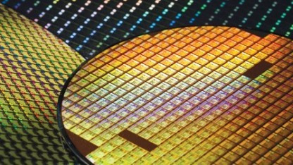
China's state-backed SMIC (Semiconductor Manufacturing International Corporation) has set an ambitious target of Q4-2020 for its 7 nanometer-class N+1 foundry node to go live, achieving "small scale production," according to a cnTechPost report. The company has a lot of weight on its shoulders as geopolitical hostility between the U.S. and China threatens to derail the country's plans to dominate 5G technology markets around the world. The SMIC N+1 node is designed to improve performance by 20%, reduce chip power consumption by 57%, reduce logic area by 63%, and reduce SoC area by 55%, in comparison to the SMIC's 14 nm FinFET node, Chinese press reports citing a statement from SMIC's co-CEO Dr. Liang Mengsong.

Dr. Liang confirmed that the N+1 7 nm node and its immediate successor will not use EUV lithography. N+1 will receive a refinement in the form of N+2, with modest chip power consumption improvement goals compared to N+1. This is similar to SMIC's 12 nm FinFET node being a refinement of its 14 nm FinFET node. Later down its lifecycle, once the company has got a handle of its EUV lithography equipment, N+2 could receive various photomasks, including a switch to EUV at scale.

Samsung Successfully Completes 5nm EUV Development

Samsung Electronics Co., Ltd., a world leader in advanced semiconductor technology, today announced that its 5-nanometer (nm) FinFET process technology is complete in its development and is now ready for customers' samples. By adding another cutting-edge node to its extreme ultraviolet (EUV)-based process offerings, Samsung is proving once again its leadership in the advanced foundry market.

Compared to 7 nm, Samsung's 5 nm FinFET process technology provides up to a 25 percent increase in logic area efficiency with 20 percent lower power consumption or 10 percent higher performance as a result of process improvement to enable us to have more innovative standard cell architecture. In addition to power performance area (PPA) improvements from 7 nm to 5 nm, customers can fully leverage Samsung's highly sophisticated EUV technology. Like its predecessor, 5 nm uses EUV lithography in metal layer patterning and reduces mask layers while providing better fidelity.

Samsung Completes Qualification of 8 nm LPP Process

Samsung Electronics announced today that their 8 nm FinFET process technology, 8LPP (Low Power Plus), has been qualified and is ready for production. Samsung's newest process node provides up to 10-percent lower power consumption with up to 10-percent area reduction from 10LPP through a narrower metal pitch. 8LPP is expected to provide benefits for applications including mobile, cryptocurrency and network/server. Samsung expects this 8 nm node to be the last feasible one with current fabrication technology - shown by the fact it's actually employing much of the same design and production processes and philosophy as the 10 nm node. Samsung is counting on EUV (Extreme Ultra Violet) technology to enable 7 nm and smaller process nodes.

"With the qualification completed three months ahead of schedule, we have commenced 8LPP production," said Ryan Lee, Vice President of Foundry Marketing at Samsung Electronics. "Samsung Foundry continues to expand its process portfolio in order to provide distinct competitive advantages and excellent manufacturability based on what our customers and the market require." Details of the recent update to Samsung's foundry roadmap, including 8LPP availability and 7nm EUV development, will be presented at the Samsung Foundry Forum Europe on October 18, 2017, in Munich, Germany.

Samsung Announces 11nm LPP and 7nm LPP With EUV Technology

Samsung Electronics Co., Ltd., the world leader in advanced semiconductor technology, today announced it has added 11-nanometer (nm) FinFET process technology (11LPP, Low Power Plus) to its advanced foundry process portfolio, offering customers with an even wider range of options for their next-generation products. Through further scaling from the earlier 14LPP process, 11LPP delivers up to 15 percent higher performance and up to 10 percent chip area reduction with the same power consumption.

In addition to the 10nm FinFET process for mobile processors in premium flagship smartphones, the company expects its 11nm process to bring differentiated value to mid- to high-end smartphones. The new process technology is scheduled to be ready for production in the first half of 2018. Samsung also confirmed that development of 7LPP with EUV (extreme ultra violet) lithography technology is on schedule, targeting its initial production in the second half of 2018.

Since 2014, Samsung has processed close to 200,000 wafers with EUV lithography technology and, building on its experience, has recently seen visible results in process development such as achieving 80 percent yield for 256 megabit (Mb) SRAM (static random-access memory).

Samsung Completes Qualification of its 2nd Generation 10nm Process Technology

Samsung Electronics Co., Ltd., a world leader in advanced semiconductor technology, announced today that its second generation 10-nanometer (nm) FinFET process technology, 10LPP (Low Power Plus), has been qualified and is ready for production. With further enhancement in 3D FinFET structure, 10LPP allows up to 10-percent higher performance or 15-percent lower power consumption compared to the first generation 10LPE (Low-Power Early) process with the same area scaling.

Samsung was the first in the industry to begin mass production of system-on-chips (SoCs) products on 10LPE last October. The latest Samsung Galaxy S8 smartphones are powered by some of these SoCs. To meet long-term demand for the 10nm process for a wide range of customers, Samsung has started installing production equipment at its newest S3-line in Hwaseong, Korea. The S3-line is expected to be ready for production by the fourth quarter of this year.

Samsung Details New Foundry Offerings at 14nm (LPU) and 10nm (LPU)

In an announcement that's sure to stir the foundry gods, Samsung Electronics, a world leader in advanced semiconductor technology, announced today that it is expanding its advanced foundry process technology offerings with the fourth-generation 14-nanometer (nm) process (14LPU) and the third-generation 10nm process (10LPU). The announcement comes as Samsung increases investment so as to meet the requirements of next generation products, ranging from mobile and consumer electronics (Snapdragon 830 and Samsung's own Exynos 8895 come to mind) to data centers and automotives.

Ben Suh, Senior Vice President of foundry marketing at Samsung Electronics, issued the following statement: "After we announced the industry's first 10nm mass production in mid-October, we have now also expanded our lineup with new foundry offerings, 14LPU and 10LPU. Samsung is very confident with our technology definitions that provide design advantages on an aggressive process with manufacturability considerations. We have received tremendous positive market feedback and are looking forward to expanding our leadership in the advanced process technology space."
Return to Keyword Browsing
May 16th, 2024 05:14 EDT change timezone

New Forum Posts

Popular Reviews

Controversial News Posts