News Posts matching #GP104

Return to Keyword Browsing

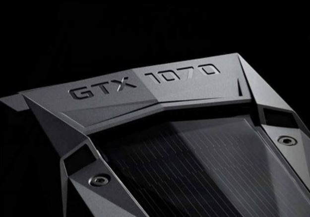
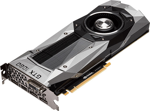
NVIDIA to Unveil GeForce GTX TITAN P at Gamescom

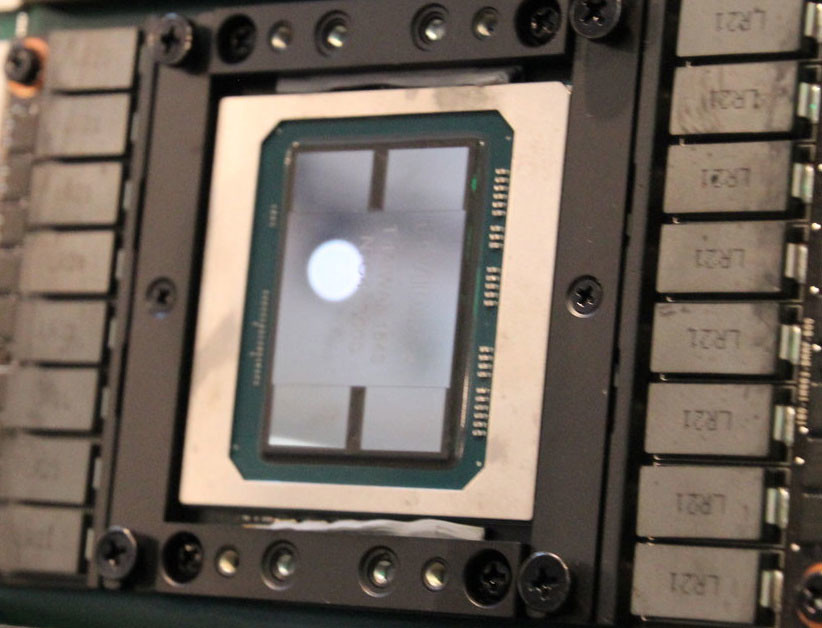
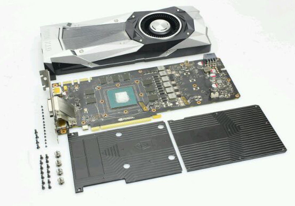
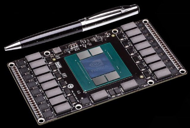
NVIDIA is preparing to launch its flagship graphics card based on the "Pascal" architecture, the so-called GeForce GTX TITAN P, at the 2016 Gamescom, held in Cologne, Germany, between 17-21 August. The card is expected to be based on the GP100 silicon, and could likely come in two variants - 16 GB and 12 GB. The two differ by memory bus width besides memory size. The 16 GB variant could feature four HBM2 stacks over a 4096-bit memory bus; while the 12 GB variant could feature three HBM2 stacks, and a 3072-bit bus. This approach by NVIDIA is identical to the way it carved out Tesla P100-based PCIe accelerators, based on this ASIC. The cards' TDP could be rated between 300-375W, drawing power from two 8-pin PCIe power connectors.

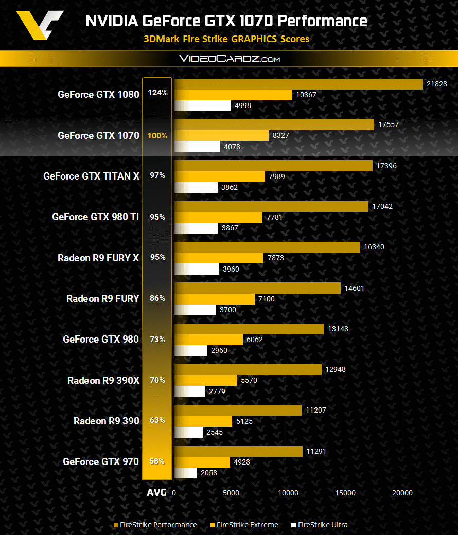
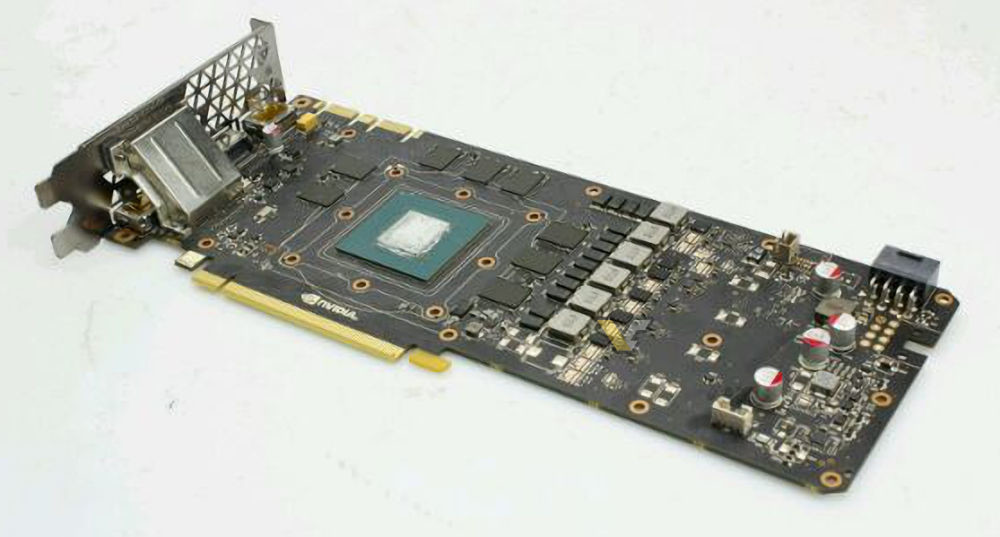
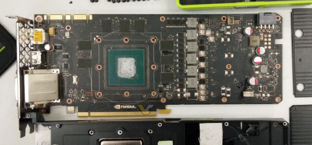
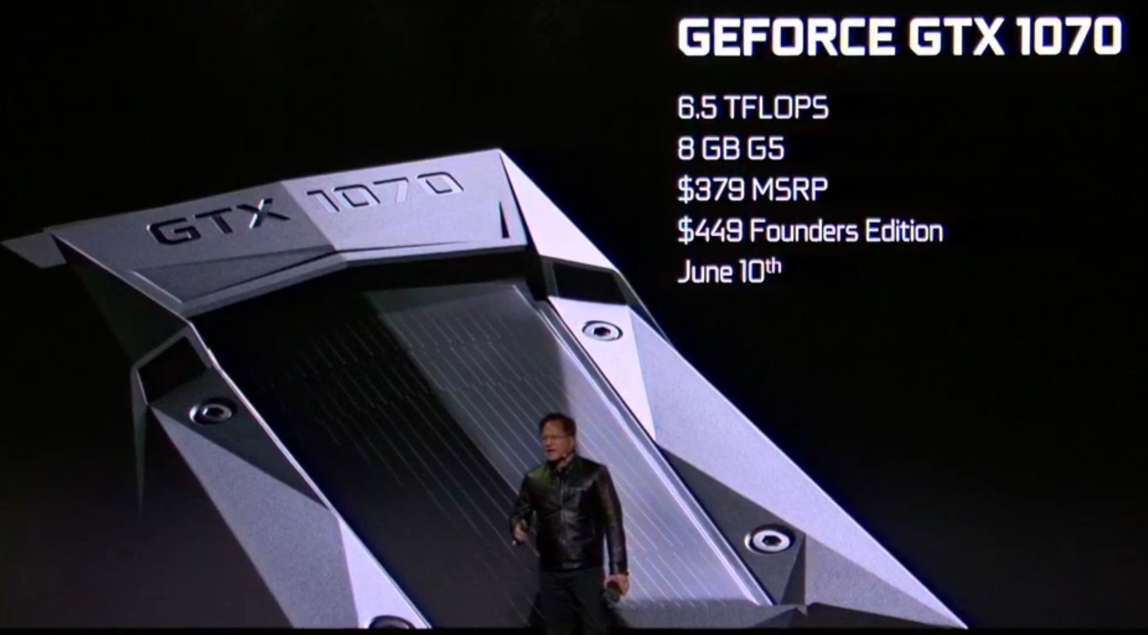
The GP100 and GTX TITAN P isn't the only high-end graphics card lineup targeted at gamers and PC enthusiasts, NVIDIA is also working the GP102 silicon, positioned between the GP104 and the GP100. This chip could lack FP64 CUDA cores found on the GP100 silicon, and feature up to 3,840 CUDA cores of the same kind found on the GP104. The GP102 is also expected to feature simpler 384-bit GDDR5X memory. NVIDIA could base the GTX 1080 Ti on this chip.

AMD "Vega 10" GPU Crosses a Development Milestone

AMD Radeon Technologies Group (RTG) chief Raja Koduri was in Shanghai last week to meet with one of the design teams of the "Polaris10" and the upcoming "Vega10." He tweeted that development of "Vega10" had just crossed a milestone, although it's a long way to go before you can see it. The 5th generation Graphics CoreNext architecture, and successor to the upcoming "Polaris" architecture, "Vega" promises a higher performance/Watt than "Polaris," which in turn boasts of a large energy efficiency leap over its predecessor.

One of the most notable derivatives of "Vega" is the "Vega10," poised to be a performance-segment GPU, which will make it to the market alongside "Vega11," a larger enthusiast-segment chip. The Vega10 is rumored to feature 4,096 stream processors spread across 64 compute units, and is expected to be a competitor to NVIDIA's GP104 silicon. The larger Vega11 could compete with larger chips based on the "Pascal" architecture, such as the GP102.

Palit Announces the GeForce GTX 1070 GameRock and JetStream Series

Palit Microsystems Ltd, the leading graphics card manufacturer, releases the latest Pascal architecture Palit GeForce GTX 1070 Series. With new technologies, GTX 1070 offers a true cinematic experience and amazing new image-capture to share your game.

The brand new gaming series, Palit "GameRock" is specially designed for enthusiast gamers who desire to have the ultimate gaming experience. GameRock series provides the best gaming features, the best thermal solution and the best graphics card quality, make you become a real game rocker without any fears. Adding RGB LED lighting feature, the color lighting from RGB LED can be changed in accordance with graphics temperature.

NVIDIA GeForce GTX 1070 Goes On Sale

NVIDIA's more economically significant graphics card based on the "Pascal" architecture, the GeForce GTX 1070, goes on sale from today (10/06). The card starts at US $379, with NVIDIA selling the reference-design board for a $70 premium, as the GTX 1070 Founders Edition, priced at $449. With NVIDIA claiming performance levels higher than the previous-generation $999 GeForce GTX Titan X, the GTX 1070 could prove to be the gateway to 4K Ultra HD gaming with reasonably high eye-candy.

Based on the 16 nm "GP104" silicon, the GeForce GTX 1070 features 1,920 CUDA cores, 120 TMUs, 64 ROPs, and a 256-bit GDDR5 memory interface, holding 8 GB of memory. The core ticks at 1506 MHz, with a GPU Boost frequency of 1683 MHz, while the memory runs at 2000 MHz (actual), 8 GHz (GDDR5-effective), yielding a memory bandwidth of 256 GB/s. Display outputs include three DisplayPort 1.4, one HDMI 2.0b, and a dual-link DVI-D.

NVIDIA GeForce GTX 1080 Ti to be Based on GP102 Silicon

It looks like NVIDIA will have not one, but two "big chips" based on the "Pascal" architecture. The first one of course is the GP100, which made its debut with the Tesla P100 HPC processor. The GP100 is an expensive chip at the outset, featuring a combination of FP32 (single-precision) and FP64 (double-precision) CUDA cores, running up to 3,840 SPFP and 1,920 DPFP, working out to a gargantuan 5,760 CUDA core count. FP64 CUDA cores are practically useless on the consumer-graphics space, particularly in the hands of gamers. The GP100 also features a swanky 4096-bit HBM2 memory interface, with stacked memory dies sitting on the GPU package, making up an expensive multi-chip module. NVIDIA also doesn't want its product development cycle to be held hostage by HBM2 market availability and yields.

NVIDIA hence thinks there's room for a middle-ground between the super-complex GP100, and the rather simple GP104, if a price-war with AMD should make it impossible to sell a GP100-based SKU at $650-ish. Enter the GP102. This ASIC will be targeted at consumer graphics, making up GeForce GTX products, including the GTX 1080 Ti. It is cost-effective, in that it does away with the FP64 CUDA cores found on the GP100, retaining just a 3,840 FP32 CUDA cores count, 33% higher than that of the GP104, just as the GM200 had 33% more CUDA cores than the GM204.

NVIDIA GeForce GTX 1070 Faster than GTX TITAN X

NVIDIA's upcoming GeForce GTX 1070 graphics card, which NVIDIA is pinning its summer upgrade revenue on, is shaping up to be faster than the previous-generation enthusiast GeForce GTX TITAN X. 3DMark FireStrike numbers scored by VideoCardz reveal that averaged across three popular resolutions - 1080p (FireStrike standard), 1440p (FireStrike Advanced), and 4K (FireStrike Ultra), the GTX 1070 is about 3 percent faster than the GTX TITAN X.

At FireStrike (standard), the GTX 1070 scored 17557 points, versus 17396 points of the GTX TITAN X; 8327 points at FireStrike Advanced against 7989; and 4078 points at FireStrike Ultra against 3862, respectively. The performance lead is highest at 4K Ultra HD. Based on the 16 nm GP104 silicon, the GeForce GTX 1070 features 1,920 CUDA cores, 120 TMUs, and 8 GB of GDDR5 memory clocked at 8.00 GHz (256 GB/s). The MSRP for this SKU is set at $379, although its reference design board will be sold at a $70 premium, for $449, when the card goes on sale this 10th June.

EK Waterblocks GeForce GTX 1080 Block Now Available

EK Water Blocks, Slovenia based premium liquid cooling gear manufacturer, is proud to introduce full-cover liquid cooling solution for NVIDIA GeForce GTX 1080 series graphics cards, based on Pascal GP104 graphics processor. EK-FC1080 GTX is a new Full-Cover water block, designed for NVIDIA GeForce GTX 1080 Founders Edition graphics cards. The block comes in four different variations and each of them directly cools the GPU, RAM as well as VRM (voltage regulation module) as water flows directly over these critical areas, thus allowing the graphics card and its VRM to remain stable under high overclocks. Performance-wise all variants of the block are the same, the only difference being the overall aesthetics. Each EK-FC1080 GTX water block covers the entire PCB of the card and with the corresponding retention backplate, users get visually stunning GPU in their system.

Every EK-FC1080 GTX water block features a central inlet split-flow cooling engine design - just like with the flagship EK-Supremacy EVO CPU water block - for best possible cooling performance. Such type of heat exchanger also works flawlessly with the reversed water flow without adversely affecting the cooling performance. Moreover, this radical design offers great hydraulic performance, allowing this product to be used in liquid cooling systems using weaker water pumps.

ASUS Teases Upcoming G Series Notebooks Powered by "Pascal" GPUs

ASUS teased an upcoming Republic of Gamers G-Series notebook. It didn't stop at the teaser pics, and went on to tease performance numbers of the untitled "GXXX" graphics processor at the heart of this beast. We'll go out on a limb here and guess that it's a new mobile GPU based on the "Pascal" architecture; more so because ASUS is claiming that it's faster than even the desktop GeForce GTX TITAN X, and has 3DMark 11 Performance-present score to show for that. ASUS plans to exhibit the notebook at the 2016 Computex; and it's becoming increasingly clear that the third GP104-based SKU promised for June 2016 could be a mobile chip after all.

NVIDIA GeForce GTX 1070 Clock Speeds Revealed

NVIDIA posted the product page of its upcoming GeForce GTX 1070 graphics card, confirming its clock-speeds, and related specifications. The card features a nominal GPU clock speed of 1506 MHz, with a maximum GPU Boost frequency of 1683 MHz. The memory is clocked at 2000 MHz (actual), or 8 GHz (GDDR5-effective), working out to a memory bandwidth of 256 GB/s. The company also rates the card's single-precision floating point performance at 6.45 TFLOP/s. Other key specs include 1,920 CUDA cores, 120 TMUs, and 64 ROPs. The GeForce GTX 1070 goes on sale, on the 10th of June, 2016.

NVIDIA GeForce GTX 1070 Specifications Revealed

NVIDIA's second graphics card based on its GP104 "Pascal" silicon, the more affordable GeForce GTX 1070, hits the shelves on June 10, 2016. At the May 7th event, the company was surprisingly quiet about its specifications, until now. It turns out that slower memory isn't the only thing setting the GTX 1070 apart from the GTX 1080. The company will also cut down the CUDA core count, a proportionate number of TMU count, and lower the GPU clock speeds.

NVIDIA set the MSRP for the GeForce GTX 1070 at US $379, $50 higher than the launch-price of the GTX 970, the most popular SKU based on the GM204 silicon. The company also plans to sell a premium reference-design card, dubbed the GeForce GTX 1070 Founders Edition, at $449, at a $70 premium. NVIDIA hopes to make the GTX 1070 the go-to card for Summer 2016 PC upgrades.
The specifications follow.

Colorful Releases its GeForce GTX 1080 Founders Edition Graphics Card

Colorful Technology Company Limited,professional manufacturer of graphics cards and motherboards, proudly debuts the world's first GeForce GTX 1080 graphics card. Announced May 6th, the new GeForce GTX 1080 will feature NVIDIA's latest GPU architecture codenamed Pascal boasting a 16nm FinFET fabrication process.

The GeForce GTX 1080 is based on the GP104 GPU armed with 2560 CUDA cores and will have a base engine clock of 1607 MHz and can boost up 1733 MHz. Complementing it will be 8 GB of GDDR5X video memory running at an effective clock rate of 10 GHz on a 256-bit bus. The GeForce GTX 1080 is designed to deliver 3x more performance than previous-generation graphics card and its breakthrough innovations in gaming give gamers new possibilities to enjoy via VR experiences.

NVIDIA GeForce GTX 1080 Reference PCB Pictured

Here are some of the first pictures of the reference GeForce GTX 1080 PCB. NVIDIA is selling the reference-design card at a $100 premium, branded as "Founders Edition." Pictures reveal the PCB to be less crowded than the GTX 980 reference PCB. The PCB appears to feature a 6-phase VRM with DrMOS chips, drawing power from a single 8-pin PCIe power connector; the 16 nm GP104 ASIC, with a smaller die than the one featured on the 28 nm GM204, neighbored by eight 8 Gbit GDDR5X memory chips, which feature smaller packages than the ones GDDR5 chips usually come in. We wish someone zoomed in on its VRM controller.

NVIDIA GeForce GTX 1080 Specifications Released

After launching its shockingly fast (claimed) GeForce GTX 1080 and GTX 1070 graphics cards, NVIDIA posted specifications of the former. The two are based on NVIDIA's swanky new 16 nm "GP104" silicon, derived from its "Pascal" GPU architecture. The architecture is detailed in our older article, here. The GeForce GTX 1080 leads the pack, featuring four graphics processing clusters, holding 2,560 CUDA cores. The core runs at a scorching 1607 MHz, with a GPU Boost frequency of 1733 MHz. In one of its demos, NVIDIA overclocked this chip to over 2100 MHz, on its reference air cooling, and the GPU barely scraped 67 °C under stress. The GTX 1080 features a 256-bit wide GDDR5X memory interface, holding 8 GB of memory. The memory is clocked at 2500 MHz (10 GHz effective), working out to a memory bandwidth of 320 GB/s.

API support includes DirectX 12 (feature-level 12_1), OpenGL 4.5, and Vulkan. Display outputs include three DisplayPort 1.4 connectors, one HDMI 2.0b, and one dual-link DVI. The reference-design card is 10.5-inch long, and double-slot. It draws power from a single 8-pin PCIe power connector, and its typical board power is rated at 180W. With the GeForce "Pascal" family, instead of caving in to DirectX 12 native multi-GPU, NVIDIA developed its SLI technology further, with the new SLI HB (high-bandwidth) bridge standard. It's essentially a 2-way bridge in which both SLI fingers of the card are used. This doubles bandwidth between the two cards, allowing higher display resolutions, and multi-display setups between high-resolution monitors. The GeForce GTX 1080 will be available from May 27, 2016, starting at US $599. The $379 GTX 1070 specifications will be revealed closer to its June 10, 2016 market availability.

NVIDIA Also Announces $379 "Faster than TITAN X" GTX 1070

Hot on the heels of the GeForce GTX 1080, the company also announced its second fastest GPU, the GeForce GTX 1070. Based on the same 16 nm GP104 silicon as the GTX 1080, the GTX 1070 features 8 GB of GDDR5 memory, and has 3 quarters the single precision performance (6.5 TFLOP/s vs. 9 TFLOP/s) of the GTX 1080. NVIDIA claims that just as the GTX 1080 is faster than the GTX 980 SLI, the GTX 1070 is faster than the GTX TITAN X, making it the second fastest GPU in existence. Available on June 10, the GTX 1070 will be priced at US $379, with a "founder's edition" (reference-design) card going for $449.

AMD Polaris 10 "Ellesmere" as Fast as GTX 980 Ti: Rumor

At a presser in Taiwan for its Radeon Pro Duo launch, AMD talked extensively about its upcoming "Polaris" and "Vega" family of GPUs. The company appears to be betting heavily on two SKUs it plans to launch this June, Polaris 10 and Polaris 11. Polaris 10 is an internal designation to Radeon R9 490(X), based on the 14 nm "Ellesmere" silicon. It may be the biggest chip AMD builds on the "Polaris" architecture, but it won't exactly be a "big chip," in that it doesn't succeed "Fiji." That honor is reserved for "Vega," which debuts in early-2017.

The "Ellesmere" silicon is more of AMD's competitor to NVIDIA's GP104. It is rumored that the R9 490(X), based on this silicon, will offer consumers performance rivaling the GeForce GTX 980 Ti (ergo faster than the Radeon R9 Fury X), at a USD $300-ish price point. "Ellesmere" will be a lean-machine, physically featuring up to 2,560 4th generation GCN stream processors (2,304 enabled on Polaris 10), a possible 256-bit GDDR5X memory interface, and a deep sub-200W typical board power rating.

New GP104 ASIC Picture Hints at GTX 1080 with GDDR5X Memory

A new picture of NVIDIA GP104 "Pascal" ASIC surrounded with GDDR5X memory chips hints at the possibility of NVIDIA reserving the new fast memory standard for the GTX 1080, and older GDDR5 for the more affordable GTX 1070. The picture reveals a GP104 chip with the ASIC code "GP104-400-A1," surrounded by eight Micron-made GDDR5X memory chips. We know from an older article that this ASIC code denotes the top-tier GTX 1080. A second picture (recently posted) reveals a "GP104-200-A1" ASIC surrounded by conventional GDDR5 memory chips. This ASIC corresponds to the second-fastest GTX 1070.

GDDR5 and GDDR5X are nearly identical electrically, and it's quite conceivable that the GP104 chip features a memory controller that supports both standards. GDDR5 can be had at speeds of up to 8 Gbps, while GDDR5X chips can range between 10 Gbps thru 12 Gbps initially, with 14 Gbps chips planned for a little later. Besides memory, CUDA core count could be another factor that sets the two SKUs apart. NVIDIA is planning to launch a total of three SKUs based on the GP104 silicon, in June 2016, beginning with the GTX 1080 and GTX 1070 in early-June (probably along the sidelines of Computex 2016), and a third SKU in mid-June.

NVIDIA GP104 "Pascal" ASIC Pictured

Here are two of the first pictures of NVIDIA's upcoming "GP104" graphics processor. This chip will drive at least three new GeForce SKUs bound for a June 2016 launch; and succeeds the GM204 silicon, which drives the current-gen GTX 980 and GTX 970. Based on the "Pascal" architecture, the GPU will be built on TSMC's latest 16 nm FinFET+ node. The chip appears to feature a 256-bit wide GDDR5 memory interface, and is rumored to feature a memory clock of 8 Gbps, yielding a memory bandwidth of 256 GB/s.

AMD's GPU Roadmap for 2016-18 Detailed

AMD finalized the GPU architecture roadmap running between 2016 and 2018. The company first detailed this at its Capsaicin Event in mid-March 2016. It sees the company's upcoming "Polaris" architecture, while making major architectural leaps over the current-generation, such as a 2.5-times performance/Watt uplift and driving the company's first 14 nanometer GPUs; being limited in its high-end graphics space presence. Polaris is rumored to drive graphics for Sony's upcoming 4K Ultra HD PlayStation, and as discrete GPUs, it will feature in only two chips - Polaris 10 "Ellesmere" and Polaris 11 "Baffin."

"Polaris" introduces several new features, such as HVEC (h.265) decode and encode hardware-acceleration, new display output standards such as DisplayPort 1.3 and HDMI 2.0; however, since neither Polaris 10 nor Polaris 11 are really "big" enthusiast chips that succeed the current "Fiji" silicon, will likely make do with current GDDR5/GDDR5X memory standards. That's not to say that Polaris 10 won't disrupt current performance-thru-enthusiast lineups, or even have the chops to take on NVIDIA's GP104. First-generation HBM limits the total memory amount to 4 GB over a 4096-bit path. Enthusiasts will have to wait until early-2017 for the introduction of the big-chip that succeeds "Fiji," which will not only leverage HBM2 to serve up vast amounts of super-fast memory; but also feature a slight architectural uplift. 2018 will see the introduction of its successor, codenamed "Navi," which features an even faster memory interface.

NVIDIA Reportedly Stops Production of Certain "Maxwell" GPUs

Paving the way for its next-generation "Pascal" architecture-based performance-thru-enthusiast GPUs, NVIDIA reportedly halted further production of certain current-generation "Maxwell" GPUs. HWBattle reports that production of the GM204-based GeForce GTX 980, the popular GTX 970, and GM200-based GTX 980 Ti have seen production halts, to let the market digest existing inventories of the three cards; and letting NVIDIA's add-in card (AIC) partners prepare to stock up next-generation graphics cards, beginning with at least three SKUs based on the GP104 silicon, in June 2016.

NVIDIA Readies Three GP104 "Pascal" Based SKUs for June 2016

NVIDIA is reportedly giving final touches to no less than three SKUs based on the 16 nm GP104 silicon, to launch some time this June. The ASIC markings for the chips that drive these SKUs are "GP104-400-A1," "GP104-200-A1" and "GP104-150-A1." If you recall, NVIDIA last reserved the "-400-A1" markings for the GeForce GTX 980 (GM204-400-A1), and the "-200-A1" for the GTX 970 (GM204-200-A1).

The GP104-150-A1 is a mystery ASIC. Either it will drive a more affordable third desktop SKU based on the GP104, or could signify a mobile SKU. The company plans to launch the products based on the GP104-400-A1 and GP104-200-A1, logical successors to the GeForce GTX 980 and GTX 970, in early June. The GP104-150-A1, on the other hand, could see the light of the day in mid-June.

NVIDIA Drive PX2 Powered by a Pair of GP106 Chips

NVIDIA's Drive PX2 compute system for self-driving cars in development, as shown at the recent GTC event hosted by the company, is driven by a pair of GP106 GPUs. On the company's consumer-graphics products, it could drive mid-thru-performance segment SKUs, succeeding the GM206 chip, which powers the GeForce GTX 960. Keeping up with the theme of "Maxwell" chips, the GP106 is expected to feature half the graphics processing clusters (GPCs) as the GP104, and its CUDA core count is expected to be closer to 1,280.

NVIDIA "Pascal" GP104 Silicon Pictured

A picture of NVIDIA's next performance-segment GPU based on the upcoming "Pascal" architecture, the GP104, was leaked to the web, revealing a heap of raw material to speculate from. To begin with, GP104 retains the traditional component layout of a simple GPU die sitting on a conventional fiberglass substrate package, with memory chips surrounding it. NVIDIA is reserving exotic specs such as stacked HBM2 memory for the high-end GP100 silicon.

Some fairly straightforward trignometry reveals that the rectangular die of the GP104 measures 15.35 mm x 19.18 mm, with one source speculating a transistor-count of 7.4-7.9 billion. The card is expected to feature 8 gigabit GDDR5 memory chips, which tick at 8 GHz (GDDR5-effective). If the memory bus width is 256-bit, then you're looking at a memory bandwidth of 256 GB/s. The CUDA core count of the GP104 could be closer to 2,560, than the 4,096 from an older report.

NVIDIA's Next Flagship Graphics Cards will be the GeForce X80 Series

With the GeForce GTX 900 series, NVIDIA has exhausted its GeForce GTX nomenclature, according to a sensational scoop from the rumor mill. Instead of going with the GTX 1000 series that has one digit too many, the company is turning the page on the GeForce GTX brand altogether. The company's next-generation high-end graphics card series will be the GeForce X80 series. Based on the performance-segment "GP104" and high-end "GP100" chips, the GeForce X80 series will consist of the performance-segment GeForce X80, the high-end GeForce X80 Ti, and the enthusiast-segment GeForce X80 TITAN.

Based on the "Pascal" architecture, the GP104 silicon is expected to feature as many as 4,096 CUDA cores. It will also feature 256 TMUs, 128 ROPs, and a GDDR5X memory interface, with 384 GB/s memory bandwidth. 6 GB could be the standard memory amount. Its texture- and pixel-fillrates are rated to be 33% higher than those of the GM200-based GeForce GTX TITAN X. The GP104 chip will be built on the 16 nm FinFET process. The TDP of this chip is rated at 175W.

NVIDIA "GP104" Silicon to Feature GDDR5X Memory Interface

It looks like NVIDIA's next GPU architecture launch will play out much like its previous two generations - launching the second biggest chip first, as a well-priced "enthusiast" SKU that outperforms the previous-generation enthusiast product, and launching the biggest chip later, as the high-end enthusiast product. The second-biggest chip based on NVIDIA's upcoming "Pascal" architecture, the "GP104," which could let NVIDIA win crucial $550 and $350 price-points, will be a lean machine. NVIDIA will design the chip to keep manufacturing costs low enough to score big in price-performance, and a potential price-war with AMD.

As part of its efforts to keep GP104 as cost-effective as possible, NVIDIA could give exotic new tech such as HBM2 memory a skip, and go with GDDR5X. Implementing GDDR5X could be straightforward and cost-effective for NVIDIA, given that it's implemented the nearly-identical GDDR5 standard on three previous generations. The new standard will double densities, and one could expect NVIDIA to build its GP104-based products with 8 GB of standard memory amounts. GDDR5X breathed a new lease of life to GDDR5, which had seen its clock speeds plateau around 7 Gbps/pin. The new standard could come in speeds of up to 10 Gbps at first, and eventually 12 Gbps and 14 Gbps. NVIDIA could reserve HBM2 for its biggest "Pascal" chip, on which it could launch its next TITAN product.

NVIDIA to Unveil "Pascal" at the 2016 Computex

NVIDIA is reportedly planning to unveil its next-generation GeForce GTX "Pascal" GPUs at the 2016 Computex show, in Taipei, scheduled for early-June. This unveiling doesn't necessarily mean market availability. SweClockers reports that problems, particularly related to NVIDIA supplier TSMC getting its 16 nm FinFET node up to speed, especially following the recent Taiwan earthquake, could delay market available to late- or even post-Summer. It remains to be seen if the "Pascal" architecture debuts as an all-mighty "GP100" chip, or a smaller, performance-segment "GP104" that will be peddled as enthusiast-segment over being faster than the current big-chip, the GM200. NVIDIA's next generation GeForce nomenclature will also be particularly interesting to look out for, given that the current lineup is already at the GTX 900 series.
Return to Keyword Browsing
May 6th, 2024 10:46 EDT change timezone

New Forum Posts

Popular Reviews

Controversial News Posts