Tuesday, April 5th 2016

NVIDIA Unveils the Tesla P100 HPC Board based on "Pascal" Architecture
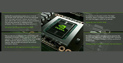
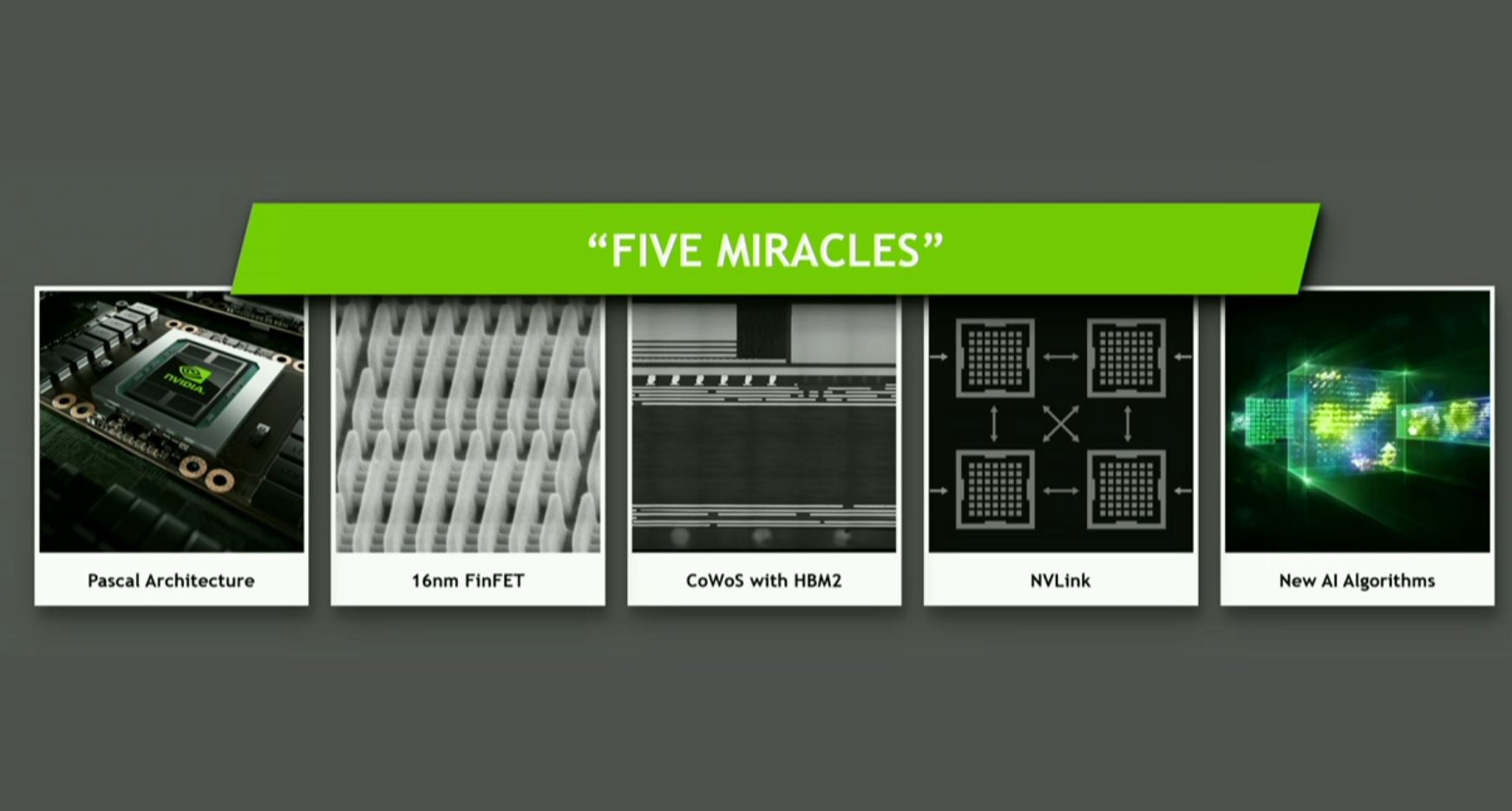
NVIDIA unveiled the Tesla P100, the first product based on the company's "Pascal" GPU architecture. At its core is a swanky new multi-chip module, similar in its essential layout to the AMD "Fiji." A 15 billion-transistor GPU die sits on top of a silicon wafer, through which a 4096-bit wide HBM2 memory interface wires it to four 3D HBM2 stacks; and with the wafer sitting on the fiberglass substrate that's rooted into the PCB over a ball-grid array. With the GPU die, wafer, and memory dies put together, this package has a cumulative transistor count of 150 billion transistors. The GPU die is built on the 16 nm FinFET process, and is 600 mm² in area.
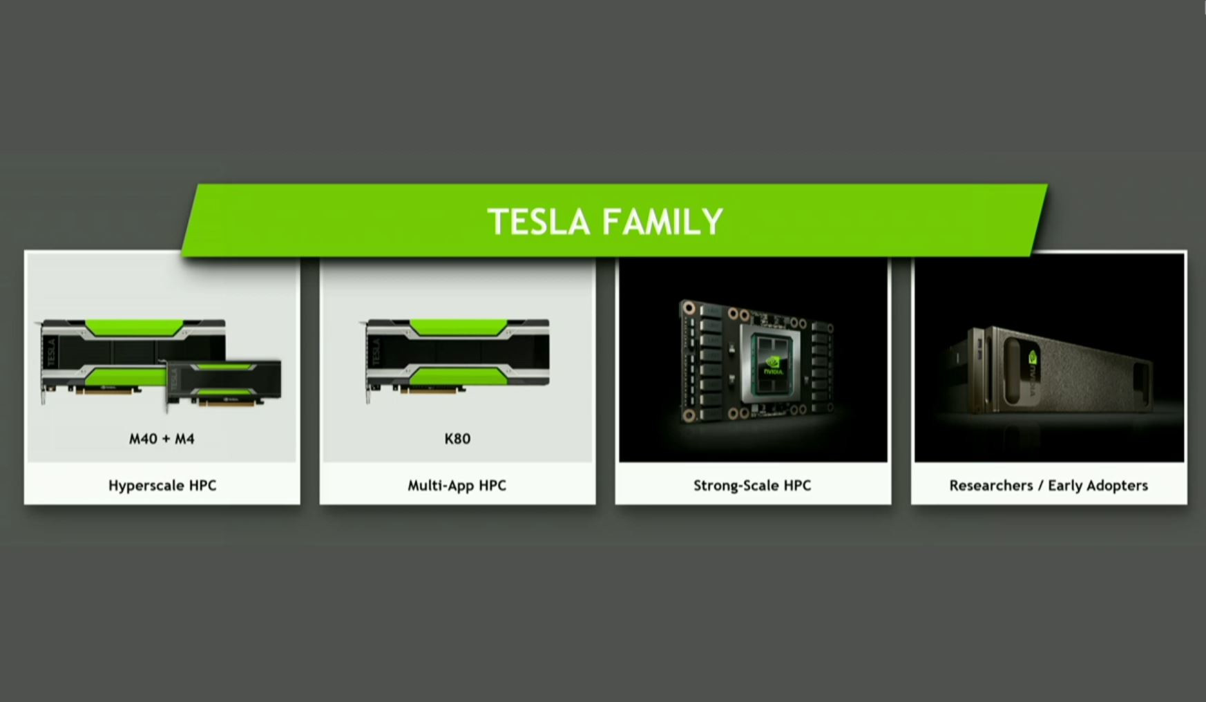
The P100 sits on top of a space-efficient PCB that looks less like a video card, and more like a compact module that can be tucked away into ultra-high density supercomputing cluster boxes, such as the new NVIDIA DGX-1. The P100 offers a double-precision (FP64) compute performance of 5.3 TFLOP/s, FP32 performance of 10.6 TFLOP/s, and FP16 performance of a whopping 21.2 TFLOP/s. The chip has registers as big as 14.2 MB, and an L2 cache of 4 MB. In addition to PCI-Express, each P100 chip will be equipped with NVLink, and in-house developed high-bandwidth interconnect by NVIDIA, with bandwidths as high as 80 GB/s per direction, 160 GB/s both directions. This allows extremely high-bandwidth paths between GPUs, so they could share memory and work more like single-GPUs. The P100 is already in volume production, with its target customers already having bought it all the way up to its OEM channel availability some time in Q1-2017.


The P100 sits on top of a space-efficient PCB that looks less like a video card, and more like a compact module that can be tucked away into ultra-high density supercomputing cluster boxes, such as the new NVIDIA DGX-1. The P100 offers a double-precision (FP64) compute performance of 5.3 TFLOP/s, FP32 performance of 10.6 TFLOP/s, and FP16 performance of a whopping 21.2 TFLOP/s. The chip has registers as big as 14.2 MB, and an L2 cache of 4 MB. In addition to PCI-Express, each P100 chip will be equipped with NVLink, and in-house developed high-bandwidth interconnect by NVIDIA, with bandwidths as high as 80 GB/s per direction, 160 GB/s both directions. This allows extremely high-bandwidth paths between GPUs, so they could share memory and work more like single-GPUs. The P100 is already in volume production, with its target customers already having bought it all the way up to its OEM channel availability some time in Q1-2017.


34 Comments on NVIDIA Unveils the Tesla P100 HPC Board based on "Pascal" Architecture
I threw up a little. Why do they have to be so.........
I'm looking forward to purchasing this top card at the affordable price that NVIDIA are known to price at and bundled with a free AAA game. :laugh:
The 150 billion figure is either a typo or they're counting all of the transistors in the HBM too.
After all, AMD did exactly the same thing with Vega at the
CapsizingCapsaicin presentation, and Intel formally unveiled Omni-Path well over a year before any interconnect hardware was sighted.devblogs.nvidia.com/parallelforall/inside-pascal/
Pretty sure, that in a few weeks, once some GTC videos make their way to Youtube, we'll get more details on what's going on + some marketing crap as usual )).
Given the conservative clocks usually associated with professional GPGPU, a near 1500MHz boost clock for a 600mm^2 augers well for the 16nmFF+ process.
Not even wooden one?
Total War: Warhammer is where it's at. DX 12 and ASYNC. And it looks like an actual game instead of a benchmark like AOS.
Anyway the HPC market is gonna lap this badboy up.
Nvidia sure is good at terrible lying.
I'm guessing that production takes into account die size/yield, HBM2 availability, and assembly yield - which are three areas that Nvidia would have virtually no control over - just as AMD had to grin and bear it with the slow Fiji ramp.
You are the one making hyperbolic claims on Nvidia's behalf. Gunning for Roy Taylor's job?
I wouldn't expect any high end gaming cards until late fall with this kind of ridiculous spin going on for PR.
Again...only you seem to be inferring that Nvidia is claiming volume production suitable for gaming cards. The company made it quite clear that wider availability of GP100 wouldn't happen until Q1 2017.
Let's see what Jen-Hsun Huang has to say:
No clue if it is faster than Tesla S."Is white a color?"
"Yes"
"Is black a color?"
"Yes"
"Told ya, I've sold you a color TV"
(A joke from times where there actually were black & white TVs)