News Posts matching #Meteor Lake

Return to Keyword Browsing

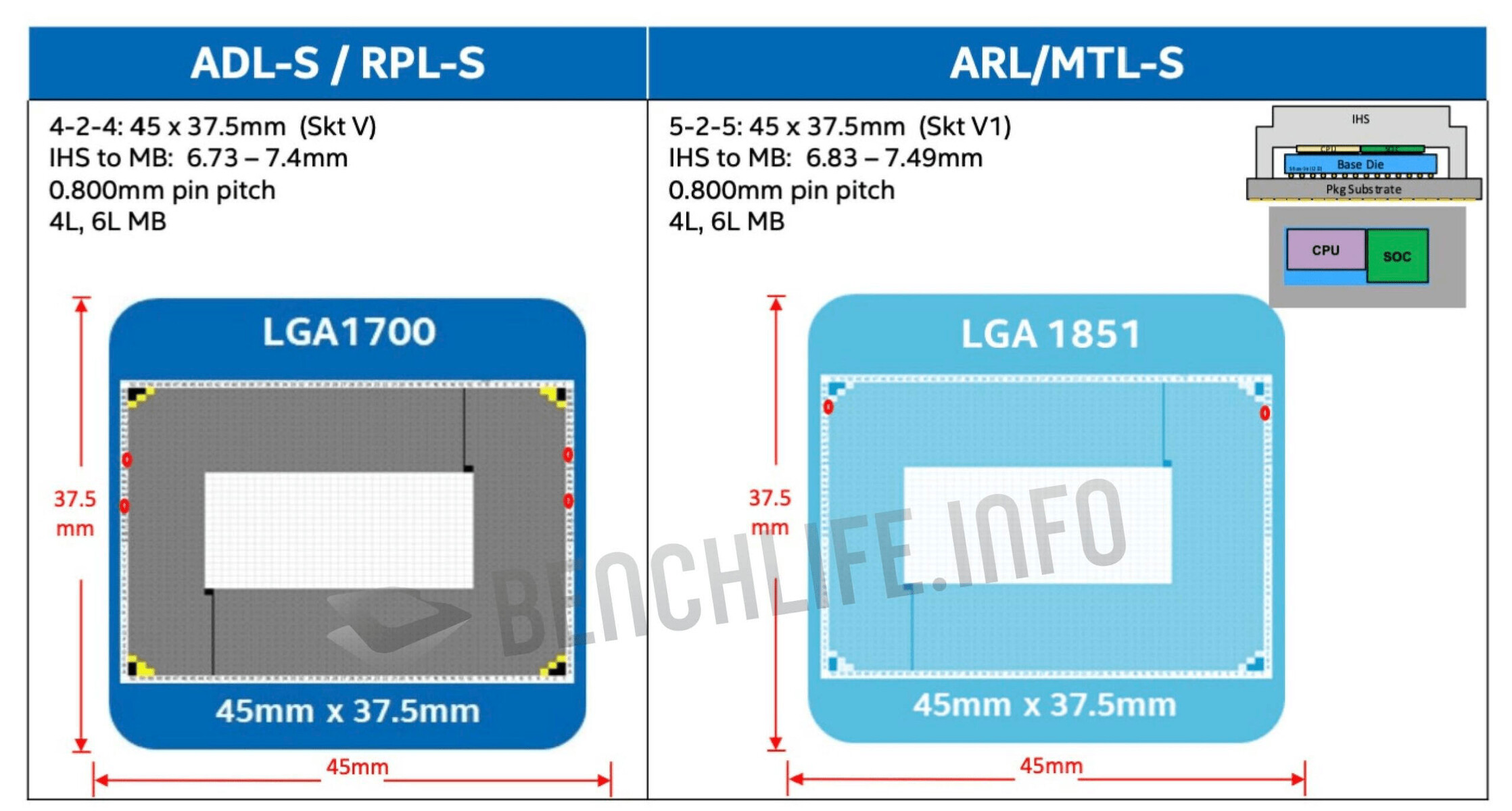
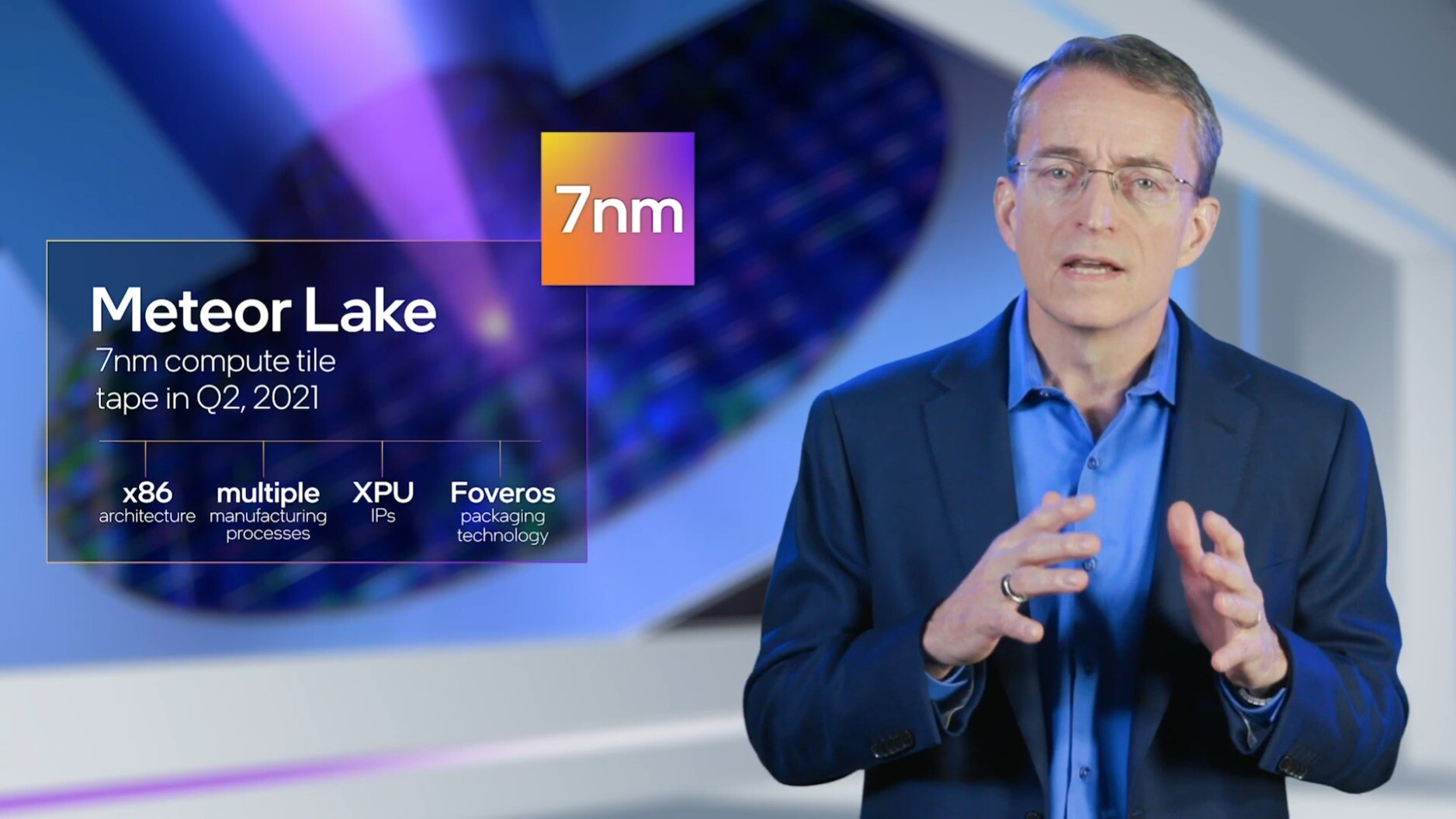
Intel "Meteor Lake-P" SoC with 6P+8E Compute Tile Pictured

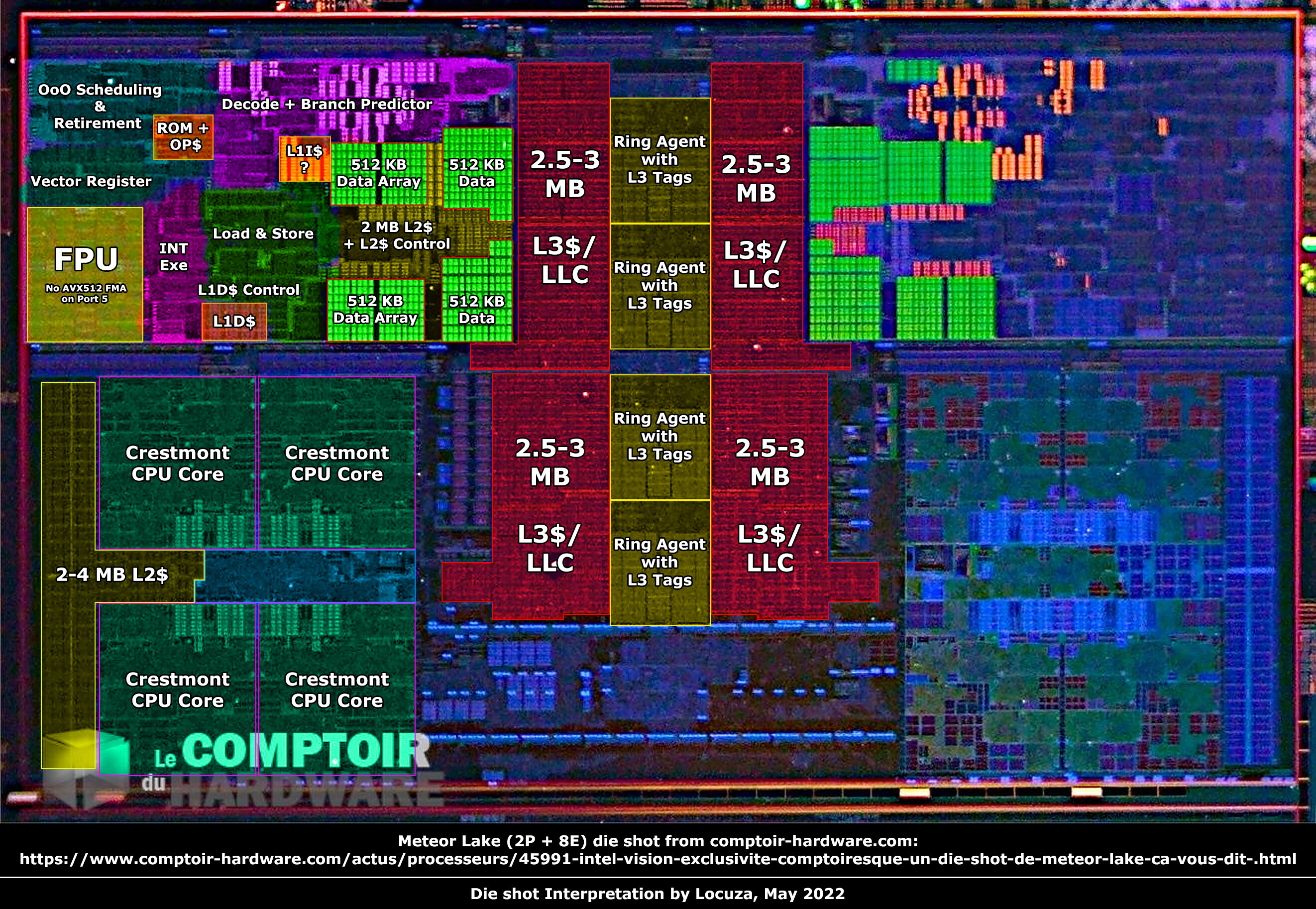
Intel's next-generation "Meteor Lake-P" mobile processor with a 6P+8E Compute Tile was shown off at the 2022 IEEE VLSI Symposium on Tech and Circuits (6 performance cores and 8 efficiency cores). We now have annotations for all four tiles, as well as a close-up die-shot of the Compute Tile. Intel also confirmed that the Compute Tile will be built on its homebrew Intel 4 silicon fabrication process, which offers over 20% iso-power performance increase versus the Intel 7 node, through extensive use of EUV lithography.

We had earlier seen a 2P+8E version of the "Meteor Lake" Compute Tile, probably from the "Meteor Lake-U" package. The larger 6P+8E Compute tile features six "Redwood Cove" performance cores, and two "Crestmont" efficiency core clusters, each with four E-cores. Assuming the L3 cache slice per P-core or E-core cluster is 2.5 MB, there has to be 20 MB of L3 cache on the compute tile. Each P-core has 2 MB of dedicated L2 cache, while each of the two E-core clusters shares 4 MB of L2 cache among four E-cores.

Intel LGA1851 to Succeed LGA1700, Probably Retain Cooler Compatibility

Intel's next-generation desktop processor socket will be the LGA1851. Leaked documents point to the next-generation socket being of identical dimensions to the current LGA1700, despite the higher pin-count, which could indicate cooler compatibility between the two sockets, much in the same way as the LGA1200 retained cooler-compatibility with prior Intel sockets tracing all the way back to the LGA1156. The current LGA1700 will service only two generations of Intel Core, the 12th Generation "Alder Lake," and the next-gen "Raptor Lake" due for later this year. "Raptor Lake" will be Intel's last desktop processor built on a monolithic silicon, as the company transitions to multi-chip modules.

Intel Socket LGA1851 will debut with the 14th Gen Core "Meteor Lake" processors due for late-2023 or 2024; and will hold out until the 15th Gen "Arrow Lake." Since "Meteor Lake" is a 3D-stacked MCM with a base tile stacked below logic tiles; the company is making adjustments to the IHS thickness to end up with an identical package thickness to the LGA1700, which would be key to cooler-compatibility, besides the socket's physical dimensions. Intel probably added pin-count to the LGA1851 by eating into the "courtyard" (the central gap in the land-grid), because the company states that the pin-pitch hasn't changed from LGA1700.

Intel to Present Meteor/Arrow Lake with Foveros 3D Packaging at Hot Chips 34

Hot Chips 34, the upcoming semiconductor conference from Sunday, August 21 to Tuesday, August 23, 2022, will feature many significant contributions from folks like Intel, AMD, Tesla, and NVIDIA. Today, thanks to Intel's registration at the event, we discovered that the company would present its work on Meteor Lake and Arrow Lake processors with the novel Foveros 3D packaging. The all-virtual presentation from Intel will include talks about Ponte Vecchio GPU and its architecture, system, and software; Meteorlake and Arrowlake 3D Client Architecture Platform with Foveros; and some Xeon D and FPGA presentations. You can see the official website here for a complete list of upcoming talks.

As a little reminder, Meteor Lake is supposed to arrive next year, replacing the upcoming Raptor Lake design, and it has already ahs been pictured, which you can see below. The presentation will be recorded and all content posted on Hot Chips's website for non-attendees to catch up on.

Intel "Meteor Lake" 2P+8E Silicon Annotated

Le Comptoir du Hardware scored a die-shot of a 2P+8E core variant of the "Meteor Lake" compute tile, and Locuza annotated it. "Meteor Lake" will be Intel's first processor to implement the company's IDM 2.0 strategy to the fullest. The processor is a multi-chip module of various tiles (chiplets), each with a certain function, sitting on die made on a silicon fabrication node most suitable to that function. Under this strategy, for example, if Intel's chip-designers calculate that the iGPU will be the most power-hungry component on the processor, followed by the CPU cores, the graphics tile will be built on a more advanced process than the compute tile. Intel's "Meteor Lake" and "Arrow Lake" processors will implement chiplets built on the Intel 4, TSMC N3, and Intel 20A fabrication nodes, each with unique power and transistor-density characteristics. Learn more about the "Meteor Lake" MCM in our older article.

The 2P+8E (2 performance cores + 8 efficiency cores) compute tile is one among many variants of compute tiles Intel will develop for the various SKUs making up the next-generation Core mobile processor series. The die is annotated with the two large "Redwood Cove" P-cores and their cache slices taking up about 35% of the die area; and the two "Crestmount" E-core clusters (each with 4 E-cores), and their cache slices, taking up the rest. The two P-cores and two E-core clusters are interconnected by a Ring Bus, and share an L3 cache. The size of each L3 cache slice is either 2.5 MB or 3 MB. At 2.5 MB, the total L3 cache will be 10 MB, and at 3 MB, it will be 12 MB. As with all past generations, the L3 cache is fully accessible by all CPU cores in the compute tile.

Intel Meteor Lake, HBM2E-enabled Sapphire Rapids, and Ponte Vecchio Pictured

Intel has allowed the media to get a closer look at the next generation of silicon that will power millions of systems in years to come during its private Vision event. PC Watch, a Japanese tech media, managed to get some shots of the upcoming Meteor Lake, Sapphire Rapids, and Ponte Vecchio processors. Starting with Meteor Lake, Intel has displayed two packages for this processor family. The first one is the ultra-compact, high-density UP9 package used for highly compact mobile systems, and it is made out of silicon with minimal packaging to save space. The second one is a traditional design with more oversized packaging, designed for typical laptop/notebook configurations.

Intel "Meteor Lake" and "Arrow Lake" Use GPU Chiplets

Intel's upcoming "Meteor Lake" and "Arrow Lake" client mobile processors introduce an interesting twist to the chiplet concept. Earlier represented in vague-looking IP blocks, new artistic impressions of the chip put out by Intel shed light on a 3-die approach not unlike the Ryzen "Vermeer" MCM that has up to two CPU core dies (CCDs) talking to a cIOD (client IO die), which handles all the SoC connectivity; Intel's design has one major difference, and that's integrated graphics. Apparently, Intel's MCM uses a GPU die sitting next to the CPU core die, and the I/O (SoC) die. Intel likes to call its chiplets "tiles," and so we'll go with that.

The Graphics tile, CPU tile, and the SoC or I/O tile, are built on three different silicon fabrication process nodes based on the degree of need for the newer process node. The nodes used are Intel 4 (optically 7 nm EUV, but with characteristics of a 5 nm-class node); Intel 20A (characteristics of 2 nm), and external TSMC N3 (3 nm) node. At this point we don't know which tile gets what. From the looks of it, the CPU tile has a hybrid CPU core architecture made up of "Redwood Cove" P-cores, and "Crestmont" E-core clusters.

Intel Updates Technology Roadmap with Data Center Processors and Game Streaming Service

At Intel's 2022 Investor Meeting, Chief Executive Officer Pat Gelsinger and Intel's business leaders outlined key elements of the company's strategy and path for long-term growth. Intel's long-term plans will capitalize on transformative growth during an era of unprecedented demand for semiconductors. Among the presentations, Intel announced product roadmaps across its major business units and key execution milestones, including: Accelerated Computing Systems and Graphics, Intel Foundry Services, Software and Advanced Technology, Network and Edge, Technology Development, More: For more from Intel's Investor Meeting 2022, including the presentations and news, please visit the Intel Newsroom and Intel.com's Investor Meeting site.

Intel "Meteor Lake" Chips Already Being Built at the Arizona Fab

With its 12th Gen Core "Alder Lake-P" mobile processors still on the horizon, Intel is already building test batches of the 14th Gen "Meteor Lake" mobile processors, at its Fab 42 facility in Chandler, Arizona. "Meteor Lake" is a multi-chip module that leverages Intel's Foveros packaging technology to combine "tiles" (purpose built dies) based on different silicon fabrication processes depending on their function and transistor-density/power requirements. It combines four distinct tiles across a single package—the compute tile, with the CPU cores; the graphics tile with the iGPU: the SoC I/O tile, which handles the processor's platform I/O; and a fourth tile, which is currently unknown. This could be a memory stack with similar functions as the HBM stacks on "Sapphire Rapids," or something entirely different.

The compute tile contains the processor's various CPU core types. The P cores are "Redwood Cove," which are two generations ahead of the current "Golden Cove." If Intel's 12-20% generational IPC uplift cadence holds, we're looking at cores with up to 30% higher IPC than "Golden Cove" (50-60% higher than "Skylake."). "Meteor Lake" also debuts Intel's next-generation E-core, codenamed "Crestmont." The compute tile is rumored to be fabricated on the Intel 4 node (optically a 7 nm-class node, but with characteristics similar to TSMC N5).

Intel Accelerates Packaging and Process Innovations

Intel Corporation today revealed one of the most detailed process and packaging technology roadmaps the company has ever provided, showcasing a series of foundational innovations that will power products through 2025 and beyond. In addition to announcing RibbonFET, its first new transistor architecture in more than a decade, and PowerVia, an industry-first new backside power delivery method, the company highlighted its planned swift adoption of next-generation extreme ultraviolet lithography (EUV), referred to as High Numerical Aperture (High NA) EUV. Intel is positioned to receive the first High NA EUV production tool in the industry.

"Building on Intel's unquestioned leadership in advanced packaging, we are accelerating our innovation roadmap to ensure we are on a clear path to process performance leadership by 2025," Intel CEO Pat Gelsinger said during the global "Intel Accelerated" webcast. "We are leveraging our unparalleled pipeline of innovation to deliver technology advances from the transistor up to the system level. Until the periodic table is exhausted, we will be relentless in our pursuit of Moore's Law and our path to innovate with the magic of silicon."

Intel LGA18XX CPU Socket Cover Pictured

The Intel LGA1700/LGA1718 sockets have featured prominently in recent leaks for the upcoming 12th Generation Core Series Alder Lake processors and their Raptor Lake successors we have seen very little mention of the LGA18XX socket. The socket cover for LGA17XX has recently been pictured and it lists also being compatible with LGA18XX which would suggest the two sockets will be somewhat similar. We don't know what products may feature the LGA18XX socket but the most likely option would be the 7 nm Meteor Lake architecture. Intel has developed a new mounting solution for the two sockets with updated hole patterns indicating they are similar.

Intel Tapes in 7nm Meteor Lake Compute Tile

Intel has today confirmed that they have taped in their upcoming 7 nm Meteor Lake compute tile meaning the design is now ready and Intel can proceed to tape out the whole chip. Intel Meteor Lake is rumored to power the 14th Gen Core series of processors which will launch in 2023 and will feature a 7 nm Enhanced SuperFin node. The Meteor Lake series of processors will be Intel's fourth product series to feature a hybrid core design and will support 600 series chipsets expected to launch later this year for 12th generation Alder Lake processors.
Gregory M. BryantGreat way to start the week! We are taping in our 7 nm Meteor Lake compute tile right now.

A well-deserved celebration by the team on this milestone.

Intel to Outsource a Part of 2023 Processor Production to TSMC

Intel's problems with processor production, especially with newer nodes like 10 nm and 7 nm, have been widely known. The company has not been able to deliver the latest semiconductor process on time and has thus delayed many product launches. However, things are looking to take a complete U-turn and the hell will freeze. During the "Intel Unleashed: Engineering the Future" webcast event that happened yesterday, the company made several announcements regarding the 7 nm process and its viability. We have already reported that the company is working on the new Meteor Lake processor lineup for 2023, supposed to be manufactured on the fixed 7 nm node.

However, it seems like Intel will have to tap external capacities to manufacture a part of its processor production. The company has confirmed that it will use an unknown TSMC process to manufacture a part of the 2023 processor lineup. That means that Intel and TSMC have already established the needed capacity and that TSMC has already booked wafer capacity for Intel. This has never happened before, as Intel always kept its processor production under the company roof. However, given that there is a huge demand for new semiconductor processes, Intel has to look at external manufacturing options to keep up with the demand.

Intel "Meteor Lake" a "Breakthrough Client Processor" Leveraging Foveros Packaging

Intel CEO Pat Gelsinger made the first official reference to the company's future-generation client processor, codenamed "Meteor Lake." Slated for market release in 2023, the processor's compute tile will be taped out in Q2-2021. Launching alongside the "Granite Rapids" enterprise processor, "Meteor Lake" will be a multi-chip module leveraging Intel's Foveros chip packaging technology.

Different components of the processor will be fabricated on different kinds of silicon fabrication nodes, and interconnected on the package using EMIB inter-die connections, or even silicon interposers. The compute tile is likely the tile containing the processor's CPU cores, and Intel confirmed a 7 nm-class foundry node for it. "Meteor Lake" will be a hybrid processor, much like the upcoming "Alder Lake," meaning that it will have two kinds of CPU cores, larger "high performance" cores that remain dormant when the machine is idling or dealing with lightweight workloads; and smaller "high efficiency" cores based on a low-power microarchitecture.

Intel "Lunar Lake" Microarchitecture Hits the Radar, Possible "Meteor Lake" Successor

Intel published Linux kernel driver patches that reference a new CPU microarchitecture, codenamed "Lunar Lake." The patch comments refer to "Lunar Lake" as a client platform, and VideoCardz predicts that it could succeed "Meteor Lake." the microarchitecture that follows "Alder Lake," which was recently announced by Intel.

Targeting both mobile and desktop platforms, "Alder Lake" will herald a new 1,700-pin LGA socket for the client desktop, and debut hybrid CPU cores on the form-factor. Expected to be built on a newer silicon fabrication node, such as the 10 nm SuperFin, the chip will combine high-performance "Golden Cove" big cores, with "Gracemont" low-power cores. Its commercial success will determine if Intel continues to take the hybrid-core approach to client processors with future "Meteor Lake" and "Lunar Lake," or whether it will have sorted out its foundry woes and build "Lunar Lake" with a homogeneous CPU core type. With "Alder Lake" expected to debut toward the end of 2021 and "Meteor Lake" [hopefully] by 2022, "Lunar Lake" would only follow by 2023-24.

Intel Starts Hardware Enablement of Meteor Lake 7 nm Architecture

In a report by Phoronix, we have the latest information about Intel's efforts to prepare the next generation of hardware for launch sometime in the future. In the latest Linux kernel patches prepared to go mainline soon, Intel has been adding support for its "Meteor Lake" processor architecture manufactured on Intel's most advanced 7 nm node. While there are no official patches in the mainline kernel yet, the first signs of Meteor Lake are expected to show up in the version 5.10, where we will be seeing the mentions of it. This way Intel is ensuring that the Meteor Lake platform will see the best software support, even though it is a few years away from the launch.

Meteor Lake is expected to debut in late 2022 or 2023, which will replace the Alder Lake platform coming soon. In a similar way to Alder Lake, Meteor Lake will use a hybrid core technology where it will combine small and big cores. The Meteor Lake platform will use the new big "Ocean Cove" design paired with small "Gracemont" cores that will be powering the CPU. This processor is going to be manufactured on Intel's 7 nm node that will be the first 7 nm design from Intel. With all the delays to the node, we are in for an interesting period to see how the company copes with it and how the design IPs turn out.

Windows 10 Scheduler Aware of "Lakefield" Hybrid Topologies, Benchmarked

A performance review of the Intel Core i5-L16G7 "Lakefield" Hybrid processor (powering a Samsung Galaxy S notebook) was recently published by Golem.de, which provides an in-depth look at Intel's ambitious new processor design that sets in motion the two new philosophies Intel will build its future processors on - packaging modularity provided by innovative new chip packaging technologies such as Foveros; and Hybrid processing, where there are two sets of CPU cores with vastly different microarchitectures and significantly different performance/Watt curves that let the processor respond to different kinds of workloads while keeping power-draw low. This concept was commercially proliferated first by Arm, with its big.LITTLE topology that took to the market around 2013. The "Lakefield" i5-L16G7 combines a high-performance "Sunny Cove" CPU core with four smaller "Tremont" cores, and Gen11 iGPU.

The Golem.de report reveals that Windows 10 thread scheduler is aware of the hybrid multi-core topology of "Lakefield," and that it is able to classify workloads at a very advanced level so the right kind of core is in use at any given time. The "Sunny Cove" core is called upon when interactive vast serial processing loads are in demand. This could even be something like launching applications, new tabs in a multi-process web-browser, or less-parallelized media encoding. The four "Tremont" cores keep the machine "cruising," handling much of the operational workload of an application, and is also better tuned to cope with highly parallelized workloads. This is similar to a hybrid automobile, where the combustion engine provides tractive effort from 0 kph, while the electric motor sustains a cruising speed.

Apple's Homebrew Mac Processor to Leverage Arm big.LITTLE

The first homebrew processor for Macs by Apple could leverage Arm big.LITTLE technology, according to a slide from a developer-relations presentation leaked by Erdi Özüağ of Donanim Haber. Apple is referring to the setup as "asymmetric cores" in its documentation, although it essentially is big.LITTLE, a technology that's been implemented by Arm SoC vendors since 2012. It combines groups of low-power (high-efficiency) and high-performance (low-efficiency) cores in response to processing demands by software, with the high-performance cores only been engaged when needed. Intel only recently introduced its rendition of this tech, called Hybrid Processing, with its Core "Lakefield" processor, and looks to scale it up with future chips such as "Meteor Lake."

Besides a multi-core big.LITTLE CPU, the Apple SoC features dedicated AI acceleration hardware, including a neural engine and matrix-multiplication hardware (dubbed ML accelerators), a dedicated video hardware encoder and decoder, and memory controller that's optimized for UMA (unified memory) for the iGPU and system memory. Apple has already started shipping Mac Mini prototypes with an Arm-based processor to its ISVs along with a special version of MacOS "Big Sur" and a wealth of software development kit to help port their x86 Mac software over to the new machine architecture.

Intel's First 7nm Client Microarchitecture is "Meteor Lake"

Intel's first client-segment processor microarchitecture built on its own 7 nm silicon fabrication process will be codenamed "Meteor Lake." The codename began surfacing in driver files and technical documents, one of which was screengrabbed and leaked to the web by Komachi Ensaka. Not much else is known about it, except that it succeeds the 10 nm++ "Alder Lake," an ambitious attempt by Intel to replicate Arm big.LITTLE heterogenous core technology on the x86 architecture, by combining a number of high-power cores with high-efficiency cores on a single piece of silicon. Intel "Lakefield," headed toward mass-production within this year, is the first such heterogenous core.

Older reports throughout 2019-20 speculate "Meteor Lake" (known at the time only by its name), could come out at a time when Intel monetizes its "Golden Cove" high-performance CPU core. It's quite likely that like "Alder Lake," it could be a heterogenous chip targeting several client form-factors, mobile and desktop. The company could leverage its 7 nm process - claimed to rival TSMC 5 nm-class in transistor density - in turning up core-counts over "Alder Lake." We'll learn more about "Meteor Lake" as we crawl toward its 2022 launch window, if it still holds up.
Return to Keyword Browsing
May 16th, 2024 12:53 EDT change timezone

New Forum Posts

Popular Reviews

Controversial News Posts