News Posts matching #PCI-Express 3.0

Return to Keyword Browsing

Intel Xeon E3 "Ivy Bridge" Processors Start Shipping in June

Intel is expected to start shipping Xeon E3 processors based on 22 nm "Ivy Bridge" silicon within June, according to a DigiTimes report. A key feature of the new Xeon chips driving its advent is support for PCI-Express 3.0, which could greatly increase bandwidth for compatible add-on cards and controllers. Ivy Bridge allows PCI-Express lanes from the processor root complex to be split into x16, x8, and even x4 links, which greatly increase bandwidth from previous-generation PCI-Express 2.0 bus. Built in the LGA1155 package, the new Xeon chips will be compatible with existing platforms that run Xeon Sandy Bridge processors, as well as new lines of server/workstation motherboards that feature PCI-Express 3.0 expansion. We know from a slightly older report that Intel will launch low-voltage Xeon processors around this time.

EVGA Announces the GeForce GTX 680 SC Signature Graphics Cards

EVGA has today officially introduced a fresh pair Kepler cards, the GeForce GTX 680 SC Signature and GeForce GTX 680 SC Signature+ which feature a 5 phase PWM design, 8-pin and 6-pin PCIe power connectors (stock models come with two 6-pin plugs), and increased frequencies - 1084 MHz (1006 MHz stock) for the base clock, 1150 MHz for the boost clock (1058 MHz) and 6208 MHz (6008 MHz) for the 2 GB of on board GDDR5 memory.

These two tweaked GTX 680s also have 1536 CUDA Cores, a 256-bit memory interface, PCI-Express 3.0 support, SLI and 3D Vision Surround capabilities, and four display outputs - two DVI, one HDMI and one DisplayPort. The GeForce GTX 680 SC Signature has a price tag of $529.99 while the GeForce GTX 680 SC Signature+, which comes equipped with a backplate, costs $549.99. Neither model is available at this time.

Sapphire Set to Launch Z77 Mainboard

SAPPHIRE Technology, a leading manufacturer and global supplier of graphics, mainboard and multimedia solutions has just announced a new mainboard developed to support the latest family of CPUs from Intel.

The SAPPHIRE Pure Platinum Z77/K is a full ATX sized board that supports the latest generation Intel i7/i5/i3 processor family using socket LGA1155. It includes full implementation of the chipset features, including multiple PCI-Express 3.0 Gen3, USB 3.0, SATA 6G and extensive I/O support. Four dual channel memory sockets are provided, supporting up to 16 GB of DDR3 memory with current technology (32 GB max when suitable modules become available).

NVIDIA GK106 GPU Detailed

Following the launch of a couple of more GK104-based SKUs, namely GeForce GTX 670 Ti, and GeForce GTX 670, some time in May; NVIDIA will launch its third (after GK104 and GK107) Kepler architecture-based silicon, codenamed GK106. GK106 will make up sub-$200 SKUs, and succeeds the GF116, on which SKUs such as the GeForce GTX 550 Ti, are based. The GK106 will make up at least one known desktop SKU, called GeForce GTX 660.

Its specifications are listed below.

Third Long PCIe Slot On High-End Z77 Boards Wired to CPU, Works Only with Ivy Bridge

It turns out that the "third" long (physical x16, electrical x4) PCI-Express slot on most higher-end Z77 chipset-based motherboards, across vendors, are wired to the CPU, and not the Z77 PCH, as the media assumed. Early buyers of these motherboards were greeted by an informative sticker stuck to the third slot, which tells them that to use the third slot, a 3rd Generation Core "Ivy Bridge" processor must be installed, although the motherboard very much supports 2nd Generation Core "Sandy Bridge" processors.

This can be explained by taking a close look at the block diagram of Intel Z77 Express system. Z77, in combination with "Ivy Bridge" processors, allows the CPU root complex to drive three devices. Its single PCI-Express x16 link can be arranged in three ways: x16/NC/NC; x8/x8/NC; and x8/x4/x4. As you can see, the third long slot is taken into the configuration. Intel figured out that since PCI-Express 3.0 x4 offers bandwidth comparable to PCI-Express 1.0 x16 to gen 3-compliant graphics cards, it's wise if the third electrical x4 slot is also wired to the CPU's PCIe root complex. This renders most high-end LGA1155 motherboards with such CPU-driven third x16 (x4) slots 3-way SLI/CrossFireX-capable. Sweet.

ZOTAC Unveils ZT-Z77-U1D SuperOverclock High-End Motherboard

ZOTAC unveiled a monster LGA1155 motherboard aimed at professional overclockers, and based on the new Intel Z77 Express chipset, the ZT-Z77-U1D. Pictured below, the designers' focus was evidently on giving the motherboard a very strong VRM, apart from just enough expansion and connectivity features for 2-way multi-GPU setups. To begin with, the LGA1155 socket is powered by a 27-phase VRM, which consists of AIO ferrite-core solid-state chokes, DrMOS, tantalum capacitors, and a super-ML multiphase capacitor to condition power. The VRM is controlled by a VRD12-compliant controller.

The LGA1155 socket is wired to four DDR3 DIMM slots, supporting dual-channel DDR3-2133+ MHz memory, and two PCI-Express 3.0 x16 slots (x8/x8, when both are populated). Other expansion slots include four PCI-Express 2.0 x1, wired to the Z77 PCH. All six SATA ports from the PCH are assigned as internal ports, that's two SATA 6 Gb/s, and four SATA 3 Gb/s. Display connectivity includes DVI, HDMI, and DisplayPort. Other connectivity includes 8+2 channel HD audio, 802.11 b/g/n, Bluetooth 3.0, gigabit Ethernet, six USB 3.0 ports (two on the rear panel, four via headers), and a number of USB 2.0 ports.

More Intel Desktop Board Media Series Motherboards Pictured

Intel activated product pages of nearly all its upcoming Desktop Board products based on 7-series chipsets. Last week, we were treated to detailed pictures of Intel's Z77 chipset-based Desktop Board products. Now we move on to other Desktop Board Media Series motherboards, those based on Intel's other 7-series client chipset the H77. Pin-compatible with Z77, Intel's H77 chipset provides nearly all features of its sibling, with the exception of overclocking. So motherboard designers needn't dedicate resources to implementing strong VRM designs on their H77 products, and can instead focus on other features such as connectivity and expansion.

Sapphire Pure Platinum Z77 Motherboard Final Iteration Pictured

Sapphire is ready with a high-end socket LGA1155 motherboard based on Intel Z77 chipset, the Pure Platinum Z77. This is Sapphire's second Z77 motherboard disclosed so far, after the Pure Black Z77 it showed us, at CES. Sapphire is offering 3-way multi-GPU support in a very unique way. Three of its four PCI-Express x16 (long) slots are wired to the CPU, all three of them PCI-Express Gen 3.0. The topmost slot is x16 and x8 capable (x8, if any of the other two slots are populated); the middle slot is x8 and x4 capable (x4, if the bottommost blue slot is populated); while the bottommost slot is x4 capable. PCI-Express 3.0 x4 offers bandwidth comparable to PCI-Express 2.0 x8 (or PCI-Express 1.1 x16), which doesn't heavily bottleneck today's graphics cards. An ingenious slot layout, made possible by inexpensive PCIe lane switches, instead of expensive bridges.

AMD Radeon HD 7990 Reference Board Pictured, Specs Confirmed in GPU-Z Screenshot

Admittedly, this is a terrible day for news on unannounced GPUs, but we rushed it in anyway. Here are the first board shots of AMD's next-generation dual-GPU graphics card, the Radeon HD 7990 (codename: "New Zealand"). Sources told us that AMD working overtime to release this SKU, to restore performance-leadership of the Radeon HD 7900 series. The dual-GPU card, according to the specifications at hand, is bearing AMD's coveted "GHz Edition" badge, its core is clocked higher than that of the HD 7970.

But first, the board shot. Pictured below is the first picture of this beast. Right away you'll question its authenticity for using a 70 mm fan instead of a lateral-flow blower, but that design change serves a purpose. Despite its high performance, the previous-generation Radeon HD 6990 was plagued with user complaints of high noise. That's because a single, normal-sized lateral-flow blower was positioned in the center, blowing through two sets of aluminum channels, at a very high speed. With the HD 7990, AMD on the other hand, borrowed the ventilation design of NVIDIA's GeForce GTX 590, to a large extant. It reused the fan found on reference-design HD 7850 and HD 7770, and placed it in middle of two heatsinks.

EVGA GeForce GTX 680 Superclocked Made Official

Only teased last week, EVGA's factory-overclocked GeForce GTX 680s are becoming a reality, with the first one to get make it out being the GTX 680 SuperClocked. The SC model is based around NVIDIA's reference design but has a base clock of 1058 MHz (1006 MHz stock), a boost clock of 1113 MHz (1058 MHz), and a memory frequency of 6208 MHz (6008 MHz).

The GeForce GTX 680 SC also packs 1536 CUDA Cores, a 256-bit memory interface, 2 GB of GDDR5 VRAM, a PCI-Express 3.0 bus interface, 3D Vision Surround and SLI support, and dual-DVI, HDMI and DisplayPort outputs.

The 'vanilla' GTX 680 SuperClocked costs $519.99 while its backplate-equipped sibling goes for $529.99. Both should become available very, very soon.

MSI B75MA-P45 Motherboard Detailed

MSI released details about its upcoming value socket LGA1155 motherboard, the B75MA-P45. MSI finds the B75 PCH a worthy option over the current-generation H61 PCH, and could hence price its B75-based motherboards competitively, to capture the entry-level LGA1155 market. The B75MA-P45 comes with out of the box support for 22 nm "Ivy Bridge" Core processors, apart from current-generation "Sandy Bridge" ones. The B75MA-P45 packs a simple 5-phase VRM to power the LGA1155 CPU. The CPU is wired to four DDR3 DIMM slots, supporting dual-channel DDR3-1600 MHz memory.

Expansion slots include one PCI-Express 3.0 x16, one PCI-Express 2.0 x1, and a legacy PCI. The legacy PCI logic is reintegrated with the PCH, and so the board doesn't use any bridge chips, further, since USB 3.0 and SATA 6 Gb/s are integrated with the PCH, MSI didn't add third-party controllers handling the two. SATA connectivity includes one SATA 6 Gb/s, and five SATA 3 Gb/s. The PCH gives out four USB 3.0 ports, two of which are found on the rear panel, two via internal header. Display connectivity includes DVI and D-Sub. 6-channel HD audio, gigabit Ethernet, and legacy PS/2 connectors complete the package. The board is driven by UEFI firmware (5 MB ME 8.0), with a graphical setup program. The B75MA-P45 is said to capture a price-point under US $100.

GeForce GTX 680 Release Driver Limits PCI-Express to Gen 2.0 on X79/SNB-E Systems

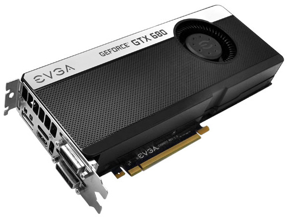
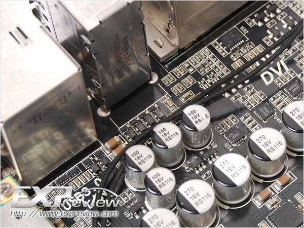
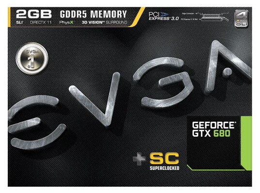
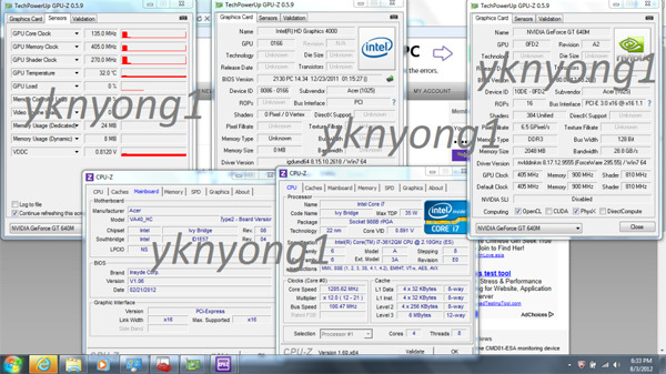
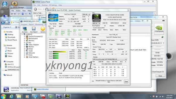
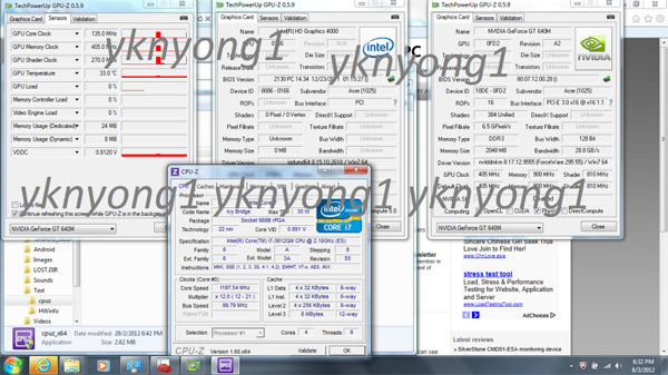
Users of systems running Core i7 processors in the LGA2011 package and X79 chipset motherboards will find that their GeForce GTX 680 will not run at PCI-Express 3.0 x16 mode, using launch drivers. This is because NVIDIA decided against implementing Gen 3.0 support for the new GPU on X79/SNB-E systems, at the very last moment. Pre-launch drivers, including the driver that ships on discs with the graphics cards, will let the GPU run at Gen 3.0 mode on some X79/SNB-E systems, however the post-launch stable drivers (such as GeForce 301.10 WHQL), won't.

The specifications page of GeForce GTX 680 on GeForce.com has been updated to mention this:
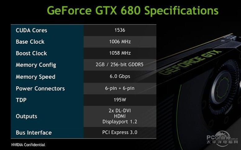
GeForce GTX 680 supports PCI Express 3.0. The Intel X79/SNB-E PCI Express 2.0 platform is only currently supported up to 5GT/s (PCIE 2.0) bus speeds even though some motherboard manufacturers have enabled higher 8GT/s speeds.
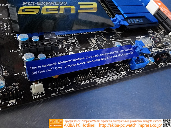
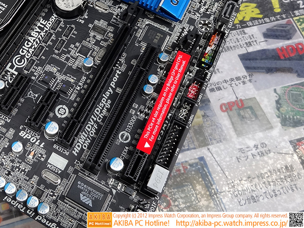
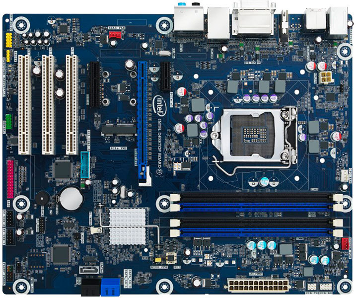
Sources in the PC motherboard industry we spoke with, confirmed this change. PCI-Express 3.0 x16, for now, might only run on upcoming "Ivy Bridge" Core systems, running on motherboards with PCI-Express 3.0 compliant components. NVIDIA could be working to fix the issue.

Update 3/23, 21:56
NVIDIA courteously responded to our article, with a statement. Here's the statement verbatim:
While X79/SNB-E is a native Gen2 platform, some motherboard manufacturers have enabled Gen3 speeds. With our GTX 680 launch drivers, we will only be supporting Gen2 speeds on X79/SNB-E while we work on validating X79/SNB-E at these faster speeds. Native Gen3 chipsets (like Ivy Bridge) will still run at full Gen3 speeds with our launch drivers.

GeForce GTX 680 supports PCI Express 3.0. It operates properly within the SIG PCI Express Specification and has been validated on multiple upcoming PCI Express 3.0 platforms. Some motherboard manufacturers have released updated SBIOS to enable the Intel X79/SNB-E PCI Express 2.0 platform to run at up to 8GT/s bus speeds. NVIDIA is currently working to validate X79/SNB-E with GTX 680 at these speeds with the goal of enabling 8GT/s via a future software update. Until this validation is complete, the GTX 680 will operate at PCIE 2.0 speeds on X79/SNB-E-based motherboards with the latest web drivers.
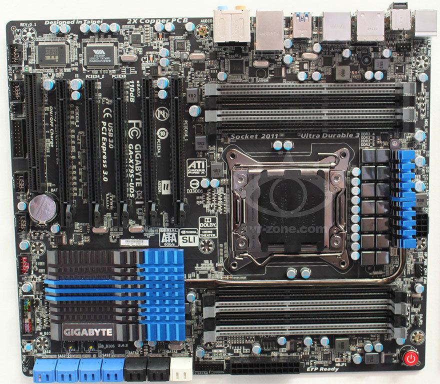
This statement confirms our assertions made in the article. NVIDIA's statement on the GeForce.com product page originally formed the basis of this article, which we pasted verbatim, while preparing the article. Motherboard manufacturers have extensively marketed their LGA2011 products as natively supporting PCI-Express Gen 3.0 (8 GT/s). What's more, the datasheet of Intel Core i7 LGA2011 processors (refer 1.2.2) clearly mentions the PCI-Express root complex as supporting 8 GT/s. AMD Southern Islands GPUs have supported PCI-Express Gen 3.0 on LGA2011 platforms since day one.

Gainward Announces its GeForce GTX 680

Palit-owned AIB maker Gainward has done as expected today by unveiling a branded GeForce GTX 680 graphics card. Seen below, the Kepler-powered card features support for DirectX 11(.1), CUDA, PhysX, 3D Vision Surround, and for 3-way SLI.

Like all the other stock GTX 680s announced today, Gainward's offering has 1536 CUDA Cores, a base GPU clock of 1006 MHz, a 256-bit memory interface, 2 GB of GDDR5 VRAM @ 6000 MHz, a PCI-Express 3.0 bus, two 6-pin PCIe power connectors, and dual-DVI, HDMI and DisplayPort outputs. The card is now available priced at €498.95.

Club 3D Comes Up with a GeForce GTX 680 Too

Dutch board maker Club 3D has today joined the Kepler launch party and announced its very own GeForce GTX 680. Based on NVIDIA's reference design, Club 3D's card is equipped with one GK104 28 nm GPU, and features 1536 CUDA Cores, a base clock of 1006 MHz, a 256-bit memory interface, and 2 GB of GDDR5 VRAM set to 6000 MHz.

The GTX 680 packs a dual-slot cooler, has 3-way SLI support, and includes four display outputs (dual DVI, HDMI and DisplayPort), PCI-Express 3.0, and goodies like Adaptive V-Sync, single-card 3D Vision Surround, TXAA, and the NVENC video encoder. The Club 3D GeForce GTX 680 can be found listed @ 487 Euro.

Point of View Introduces its GeForce GTX 680

Point of View, a premier NVIDIA graphics partner and manufacturer of Android tablets, notebooks and other hardware, launches today the first card of the GeForce 600 family: the POV GeForce GTX 680.

Current gen games have become more beautiful with higher poly meshes, larger textures and better shading technologies. In their quest for realism, game developers have demanded that we push graphics technologies to the limit.

The DirectX 11 and shader model 5.0 supporting GeForce GTX 680 is unlike any graphics card you've seen so far, performance wise and feature wise!

MSI Slips Out Some GeForce GTX 680 Marketing Material

NVIDIA's GeForce GTX 680 is certainly generating a lot of excitement, so much so that one AIB maker, MSI, has jumped the gun and put out a few PR goodies relating to the incoming card. Seen below, MSI's marketing materials show off the company's GTX 680 (which is based on NVIDIA's reference design), the new GEFORCE GTX logo, and some specs and features like the 2 GB of GDDR5 VRAM, the 256-bit memory interface, the quad display outputs, the PCI-Express 3.0 support, and the ability to run four monitors (and a complete 3D Vision Surround setup) from a single card.

MSI's GeForce GTX 680 will also be fully supported by the company's Afterburner utility that's set to provide 'GPU/Memory Clock Offset and Power Limit Control'. Expect an official unveiling of the MSI GeForce GTX 680 this Thursday, March 22nd.

- pictures removed at MSI's request -

Gigabyte Officially Launches Radeon HD 7800 Overclock Series Graphics Cards

GIGABYTE Technology Co. LTD., a leading manufacturer of motherboards and graphics cards, is pleased to present Radeon HD 7800 Overclock Series Graphics Card: GV-R787OC-2GD, GV-R785OC-2GD. Built with AMD's latest 28nm GPU and GDDR5 memory, GIGABYTE makes these cards with higher core clock. Equipped with GIGABYTE's latest in-house cooling design and adapted with GIGABYTE Ultra Durable materials, GIGABYTE makes sure that Radeon HD 7800 Series is with the best speed of heat dissipation and performance.

GIGABYTE Radeon HD 7800 Series also provides a number of innovative features including the latest AMD APP Acceleration, Microsoft DirectX 11 supported, AMDHD3D, Crossfire, and PCI-Express 3.0 supported. GIGABYTE GV-R787OC-2GD, GV-R785OC-2GD, guarantee gamers to have the best gaming experience with realistic visuals and fantastic gaming performance.

Optical Thunderbolt IO Arriving This Year

Intel's 10 Gbps Thunderbolt IO was originally pitched to be a photonic (fiber-optic) data interconnect, when it was codenamed "Lightpeak". The company managed to achieve acceptable, and comparable bandwidths over copper wire, and hence the electronic variant of the interconnect was introduced to the market in February, 2011. The copper-wire version of Thunderbolt can sustain 10 Gbps bandwidths only up to a distance of 6 meters, it was still favoured probably because electronic physical-layer PHYs are cheaper to produce than photonic ones, and that electronic cables can also transmit power (10W of it).

The fiber optic version of Thunderbolt is still taking shape, and Intel believes optical cables for Thunderbolt could be out in 2012. The fiber optic cable loses the ability to transmit power, but can sustain high bandwidths over greater distances, "tens of meters," enabling longer cables. Intel did not give out a tentative date for the launch of optical Thunderbolt, but it could be linked to several other developments, such as the propagation of PCI-Express 3.0, which provides a generous 2000 MB/s per lane of system bandwidth.

GeForce GTX 680 Specifications Sheet Leaked

Chinese media site PCOnline.com.cn released what it claims to be an except from the press-deck of NVIDIA's GeForce GTX 680 launch, reportedly scheduled for March 22. The specs sheet is in tune with a lot of information that we already came across on the internet, when preparing our older reports. To begin with the GeForce GTX 680 features clock speeds of 1006 MHz (base), and 1058 MHz (boost). The memory is clocked at a stellar 6.00 GHz (1500 MHz actual), with a memory bus width of 256-bit, it should churn out memory bandwidth of 192 GB/s. 2 GB is the standard memory amount.

For the umpteenth time, this GPU does feature 1,536 CUDA cores. The card draws power from two 6-pin PCIe power connectors. The GPU's TDP is rated at 195W. Display outputs include two DVI, and one each of HDMI and DisplayPort. Like with the new-generation GPUs from AMD, it supports PCI-Express 3.0 x16 bus interface, which could particularly benefit Ivy Bridge and Sandy Bridge-E systems, in cases where the link width is reduced to PCI-Express 3.0 x8 when there are multiple graphics cards installed.

New NVIDIA GeForce GTX 680 Pictures Hit The Web

Courtesy of ChipHell we now have a couple of fresh pictures of NVIDIA's first Kepler-powered graphics card, the GeForce (or should we write' GeFORCE') GTX 680. Shot both from above and the back, the incoming card has a black PCB, a dual-slot/single-fan cooler, two (stacked) 6-pin PCIe power plugs, a couple of SLI connectors, and four display outputs - dual DVI, HDMI and DisplayPort.

The GTX 680 is equipped with one GK104 28 nm GPU, and reportedly boasts 1536 CUDA Cores, a 256-bit memory interface, 2 GB of GDDR5 VRAM (4 GB models should also be in the works), PCI-Express 3.0, and a TDP of around 190 W. The GeForce GTX 680 is expected to be launched next week, on March 22nd. Its rumored price tag is $549.

Acer VA40 Combines Core i7-3612QM and GeForce GT 640M

NVIDIA's Kepler and Intel's Ivy Bridge architectures are a match made in Acer's upcoming VA40 notebook. The notebook combines Intel Core i7-3612QM quad-core processor with NVIDIA GeForce GT 640M discrete graphics, and with NVIDIA Optimus technology, performs dynamic-switching between the GT 640M and Intel HD 4000 graphics embedded into the processor. A Chinese forum user "yknyong1" posted screenshots of the two components using available diagnostic software. We know that CPU-Z 1.6 adds reliable support for Ivy Bridge CPUs, but GPU-Z 0.5.9 has preliminary support for Kepler GPUs, too. At least it knows how to count CUDA cores, ROPs, clock-speeds, and other basic information, even if it gets a few other details inaccurate. Kepler support will be refined and made reliable days ahead of NVIDIA's big launch day, later this month.

The Core i7-3612QM is a quad-core chip clocked at 2.10 GHz, featuring 6 MB L3 cache of the Ivy Bridge silicon, and HyperThreading, which enables 8 logical CPUs. The GeForce GT 640M, on the other hand, is known to be based on NVIDIA's new 28 nm GK107 silicon. It is detected with 384 CUDA cores, 2 GB of DDR3 memory over a 128-bit wide memory interface, 16 ROPs, core clock speed of 405 MHz, and 900 MHz memory. The chip carries a device ID of 10DE-0FD2, and is compliant with PCI-Express 3.0 bus interface. When on light load (desktop), the clock speeds of this GPU were turned down to 135 MHz core with 405 MHz memory. Find more barely-legible screenshots at the source.

ASUS Makes Z9PE-D8 WS 2P-LGA2011 Motherboard Official

ASUS made its workstation-grade Z9PE-D8 WS motherboard official. The board is built for 2P Xeon E5-2600 series processors in the LGA2011 package, is based on the Intel C606 "Patsburg" chipset, and is built in the 30.5 x 33 cm EEB form-factor. Each of the two sockets is wired to four DDR3 DIMM slots, supporting quad-channel memory, each. Up to 256 GB of registered DDR3 memory is supported.

Expansion slots include four PCI-Express 3.0 x16 (blue), two PCI-Express 3.0 x16 (electrical x8, top two black), and one PCI-Express 2.0 x16 (electrical x4, bottommost black). 4-way SLI and CrossFireX are supported. Storage connectivity includes six SATA 6 Gb/s (two from the PCH, four from two Marvell 9230 chips), and eight SATA 3 Gb/s (all from the PCH). An ASPEED ASMB6 provides basic display and iKVM functions. Realtek ALC898 provides 8-channel HD audio. There are two gigabit Ethernet interfaces, driven by Intel 82574L chips. The Z9PE-D8 WS from ASUS is priced around US $630.

Gigabyte Unveils X79S-UD5 Workstation Motherboard

At CeBIT, Gigabyte unveiled what many may have overlooked for bearing a strong resemblance to the GA-X79-UD5, the GA-X79S-UD5. This board is designed to be a 1P workstation-grade motherboard, probably with out of the box support for the latest Xeon processors in the LGA2011 package, apart from Core i7 ones. The upper-half of this board is nearly identical to that of the X79-UD5. The LGA2011 CPU is powered by a 14-phase VRM, wired to eight DDR3 DIMM slots (two on either sides), supporting quad-channel memory. There are minor differences (as far as the upper-half is concerned). Tantulum capacitors on the X79-UD5 are replaced with cylindrical solid-state ones on the X79S-UD5, the FrescoLogic-made USB 3.0 controller is replaced with a VLI-made one.

It's the lower half of the X79S-UD5, where all the action is. The expansion slot load-out consists of five long PCI-Express x16 slots. Among these, two are PCI-Express 3.0 x16 capable, one is PCI-Express 3.0 x8 capable (by taking 8 lanes from one of the two x16 links), and two appear to be PCI-Express 2.0 x4. Then there's a legacy PCI slot. The PCH heatsink is identical to the one on the X79-UD5, but what's under it is what counts. Although named "X79"S-UD5, the board is actually based on the Intel C606 "Patsburg", which is an enterprise-grade chipset for Intel's Sandy Bridge-EP platforms. Apart from six SATA ports (2x 6 Gb/s + 4x 3 Gb/s), the C606 PCH provides eight SAS (Serial-attached SCSI) ports, running at 3 Gb/s speeds. The rest of the connectivity is completely identical to that of the X79-UD5.

ECS Z77H2-A3 Detailed

Apart from the two Black Extreme models based on the Z77 chipset, ECS also has a value ATX motherboard that will capture a key sub-$150 price point, the Z77H2-A3. It is designed for single graphics cards, and lends the platform with all the connectivity and overclocking capabilities of the Z77 chipset. The CPU is powered by a simple 6-phase VRM, although the PCB is narrow (305 x 210 mm), there's room for four DDR3 DIMM slots. Expansion slots include one PCI-Express 3.0 x16, four PCIe x1, and two PCI.

The Z77H2-A3 doesn't add much features beyond what the chipset does. There are two SATA 6 Gb/s, four SATA 3 Gb/s, 8-channel HD audio, gigabit Ethernet, display connectivity that includes D-Sub, DVI/HDMI (variants), and four USB 3.0 ports (two on the rear-panel, two via headers). UEFI with graphical setup program and ECS EZ-Charger come standard.

Shuttle's Z77-based XPC Z77R5 Pictured

Shuttle unveiled the XPC Z77R5 mini-PC barebone at CeBIT. It is built into a familiar-looking XPC chassis, but with a new motherboard based on the Intel Z77 chipset, which lends it support for "Ivy Bridge" Core i7/i5/i3 processors out of the box, apart from support for LGA1155 "Sandy Bridge" processors. Connectors include six USB 2.0, four USB 3.0, HDMI, DVI, RJ-45 (gigabit Ethernet), 2x SATA 6 Gb/s, eSATA, and 8-ch HD audio. There are four expansion slots, one PCI-Express 3.0 x16, one PCI-Express 2.0 x4, and two mini-PCIe.

The chassis includes drive bays for 1 5.25" drive (such as optical drives), two internal+exposed 3.5" bays, for gadgets such as card readers. The power supply is rated at 500W, with 80 Plus Bronze efficiency rating. The XPC Z77R5 chassis measures 32.5 x 21.5 x 19.8 cm (DxWxH). Pricing and availability information was not given out.
Return to Keyword Browsing
May 21st, 2024 15:38 EDT change timezone

New Forum Posts

Popular Reviews

Controversial News Posts