News Posts matching #TSMC

Return to Keyword Browsing

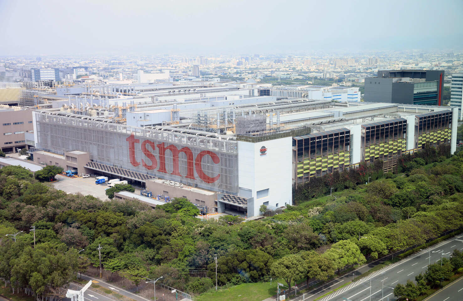
TSMC Planning Advanced Packaging Capacity Expansion due to Increased Demand for NVIDIA AI Tech

TSMC is quickly reacting to a surge in demand for NVIDIA hardware following an AI industry boom - the Taiwanese semiconductor contract manufacturer is reportedly planning to further expand its advanced packaging capabilities, due to current production lines hitting maximum capacity. News outlets have also cited the growth of 5G technology and Internet of Things (IoT) device markets as contributing factors. DigiTimes Asia reports that clients are snapping up chip-on-wafer-on-substrate (CoWoS) at an increased and unprecedented rate. TSMC has decided to provide NVIDIA - an extremely high profile customer - with an extra 10,000 CoWoS wafers. The article sourced information from a recent company shareholder meeting, where chairman Mark Liu discussed these expansions plans. He outlined improved factory facilities that will result in an additional output of 1,000 to 2,000 wafers per month. TSMC is set to upgrade equipment at its existing facilities in order to meet increasing demand.

Trendforce has also published its evaluation from the same TSMC shareholding meeting: "Due to the generative AI trend initiated by ChatGPT, the demand for advanced packaging orders for TSMC has increased, forcing an increase in advanced packaging capacity. TSMC also pointed out that the demand for TSMC's advanced packaging capacity far exceeds the existing capacity, and it is forced to increase production as quickly as possible. Chairman Mark Liu stated that the current investment in R&D focuses on two legs, namely 3D IC (chip stacking) and advanced packaging...At present, three-quarters of TSMC's R&D expenditure is used for advanced processes, and one quarter for mature and special processes, with advanced packaging falling under mature and special processes."

TSMC Employees Experiencing Problems in Arizona

TSMC is having a tough time establishing itself in the United States with new manufacturing facilities - the Taiwanese multinational semiconductor contract manufacturing and design company is putting a great deal of effort into finishing its new Arizona foundry, located in the greater Phoenix area. A minor fire incident occurred at one of their construction sites in late April, and North American news outlets last week reported on the company's struggle to recruit enough staff - approximately 4500 positions - for its upcoming Arizona plants. Current and former employees of TSMC in the U.S. have taken to the Glassdoor review website - user feedback has so far awarded the company a 27% approval rating via 91 submissions, thus warning potential candidates to stay away. Apparently American staffers have found it difficult to adjust to TSMC's corporate culture, and the company could face further challenges when transferring staff from Taiwan.

The latest news from Arizona points to problems encountered at the so-called "TSMC Village" - actually two residential locations divided into "A" and "B" categories. Taiwan's Economic Daily released a video report late last month covering crime-related incidents - this information has since been picked up by Western news outlets. Perpetrators have targeted houses and cars within these new build communities - UDN's footage indicates that seven vehicles located in Village A were damaged with a portion of them broken into. A single Village B property was accessed by possible squatters, and an unspecified number of TSMC engineers have been "robbed" throughout May. Several residents were contacted by UDN - interviewees expressed frustrations with the lack of security in the area, and blamed a local management company for not bolstering prevention measures.

TSMC N3 Nodes Show SRAM Scaling is Hitting the Wall

When TSMC introduced its N3 lineup of nodes, the company only talked about the logic scaling of the two new semiconductor manufacturing steps. However, it turns out that there was a reason for it, as WikiChip confirms that the SRAM bit cells of N3 nodes are almost identical to the SRAM bit cells of N5 nodes. At TSMC 2023 Technology Symposium, TSMC presented additional details about its N3 node lineup, including logic and SRAM density. For starters, the N3 node is TSMC's "3 nm" node family that has two products: a Base N3 node (N3B) and an Enhanced N3 node (N3E). The base N3B uses a new (for TSMC) self-aligned contact (SAC) scheme that Intel introduced back in 2011 with a 22 nm node, which improves the node's yield.

Regardless of N3's logic density improvements compared to the "last-generation" N5, the SRAM density is almost identical. Initially, TSMC claimed N3B SRAM density was 1.2x over the N5 process. However, recent information shows that the actual SRAM density is merely a 5% difference. With SRAM taking a large portion of the transistor and area budget of a processor, N3B's soaring manufacturing costs are harder to justify when there is almost no area improvement. For some time, SRAM scaling wasn't following logic scaling; however, the two have now completely decoupled.

Arm Launches the Cortex-X4, A720 and A520, Immortalis-G715 GPU

Mobile devices touch every aspect of our digital lives. In the palm of your hand is the ability to both create and consume increasingly immersive, AI-accelerated experiences that continue to drive the need for more compute. Arm is at the heart of many of these, bringing unlimited delight, productivity and success to more people than ever. Every year we build foundational platforms designed to meet these increasing compute demands, with a relentless focus on high performance and efficiency. Working closely with our broader ecosystem, we're delivering the performance, efficiency and intelligence needed on every generation of consumer device to expand our digital lifestyles.

Today we are announcing Arm Total Compute Solutions 2023 (TCS23), which will be the platform for mobile computing, offering our best ever premium solution for smartphones. TCS23 delivers a complete package of the latest IP designed and optimized for specific workloads to work seamlessly together as a complete system. This includes a new world-class Arm Immortalis GPU based on our brand-new 5th Generation GPU architecture for ultimate visual experiences, a new cluster of Armv9 CPUs that continue our performance leadership for next-gen artificial intelligence (AI), and new enhancements to deliver more accessible software for the millions of Arm developers.

TSMC CFET Transistors in the Lab, Still Many Generations Away

During the European Technology Symposium 2023, TSMC presented additional details regarding the upcoming complementary FET (CFET) technology to power the next generation of silicon-based devices. With Nanosheet replacing FinFET, the CFET technology will do the same to the Gate All Around FET (GAAFET) Nanosheet nodes. As the company notes, CFET transistors are now in the TSMC labs and are being tested for performance, efficiency, and density. Compared to GAAFET, CFET will provide greater design in all of those areas, but it will require some additional manufacturing steps to get the chip working as intended. Integrating both p-type and n-type FETs into a single device, CFET will require the use of High NA EUV scanners with high precision and high power to manufacture it.

The use of CFET, as the roadmap shows, is one of the last steps in the world of silicon. It will require the integration of new materials into the manufacturing process, resulting in a greater investment into research and development that is in charge of node creation. Kevin Zhang, senior vice president at TSMC, responsible for technology roadmap and business development, notes: "Let me make a clarification on that roadmap, everything beyond the Nanosheet is something we will put on our [roadmap] to tell you there is still future out there. We will continue to work on different options. I also have the add on to the one-dimensional material-[based transistors] […], all of those are being researched on being investigated on the future potential candidates right now, we will not tell you exactly the transistor architecture will be beyond the Nanosheet."

Artificial Intelligence Helped Tape Out More than 200 Chips

In its recent Second Quarter of the Fiscal Year 2023 conference, Synopsys issued interesting information about the recent moves of chip developers and their usage of artificial intelligence. As the call notes, over 200+ chips have been taped out using Synopsys DSO.ai place-and-route (PnR) tool, making it a successful commercially proven AI chip design tool. The DSO.ai uses AI to optimize the placement and routing of the chip's transistors so that the layout is compact and efficient with regard to the strict timing constraints of the modern chip. According to Aart J. de Geus, CEO of Synopsys, "By the end of 2022, adoption, including 9 of the top 10 semiconductor vendors have moved forward at great speed with 100 AI-driven commercial tape-outs. Today, the tally is well over 200 and continues to increase at a very fast clip as the industry broadly adopts AI for design from Synopsys."

This is an interesting fact that means that customers are seeing the benefits of AI-assisted tools like DSO.ai. However, the company is not stopping there, and a whole suite of tools is getting an AI makeover. "We unveiled the industry's first full-stack AI-driven EDA suite, sydnopsys.ai," noted the CEO, adding that "Specifically, in parallel to second-generation advances in DSO.ai we announced VSO.ai, which stands for verification space optimization; and TSO.ai, test space optimization. In addition, we are extending AI across the design stack to include analog design and manufacturing." Synopsys' partners in this include NVIDIA, TSMC, MediaTek, Renesas, and IBM Research, all of which used AI-assisted tools for chip design efforts. A much wider range of industry players is expected to adopt these tools as chip design costs continue to soar as we scale the nodes down. With future 3 nm GPU costing an estimated $1.5 billion, 40% of that will account for software, and Synopsys plans to take a cut in that percentage.

India Homegrown HPC Processor Arrives to Power Nation's Exascale Supercomputer

With more countries creating initiatives to develop homegrown processors capable of powering powerful supercomputing facilities, India has just presented its development milestone with Aum HPC. Thanks to information from the report by The Next Platform, we learn that India has developed a processor for powering its exascale high-performance computing (HPC) system. Called Aum HPC, the CPU was developed by the National Supercomputing Mission of the Indian government, which funded the Indian Institute of Science, the Department of Science and Technology, the Ministry of Electronics and Information Technology, and C-DAC to design and manufacture the Aum HPC processors and create strong, strong technology independence.

The Aum HPC is based on Armv8.4 CPU ISA and represents a chiplet processor. Each compute chiplet features 48 Arm Zeus Cores based on Neoverse V1 IP, so with two chiplets, the processor has 96 cores in total. Each core gets 1 MB of level two cache and 1 MB of system cache, for 96 MB L2 cache and 96 MB system cache in total. For memory, the processor uses 16-channel 32-bit DDR5-5200 with a bandwidth of 332.8 GB/s. To expand on that, HBM memory is present, and there is 64 GB of HBM3 with four controllers capable of achieving a bandwidth of 2.87 TB/s. As far as connectivity, the Aum HPC processor has 64 PCIe Gen 5 Lanes with CXL enabled. It is manufactured on a 5 nm node from TSMC. With a 3.0 GHz typical and 3.5+ GHz turbo frequency, the Aum HPC processor is rated for a TDP of 300 Watts. It is capable of producing 4.6+ TeraFLOPS per socket. Below are illustrations and tables comparing Aum HPC to Fujitsy A64FX, another Arm HPC-focused design.

Apple M3 Pro Chip to Pack Entry-Level Configuration of 12 CPU Cores and 18 GPU Cores on TSMC 3 nm Technology

Thanks to the latest release of the Power On newsletter from Mark Gurman, we have additional information about Apple's upcoming M3 Pro chip. Currently in testing and reported on by an App Store developer, Apple is looking to upgrade the microarchitecture of the forthcoming chip and add additional cores to the system for more performance. As the report notes, the entry-level M3 Pro chip currently in testing will have 12 CPU cores, six for efficiency and six for performance tasks, with 18 graphics cores, all manufactured on TSMC's 3 nm node. The current baseline for M2 Pro is 10 CPU cores, where four are dedicated to efficiency, and six are dedicated to performance. The current generation entry-level M2 Pro also features a 16-core GPU, which is two cores fewer than the upcoming model.

Generally, the M3 Pro chip will boost integrated memory across the board, as the sample spotted in testing shows 36 GB of memory. The M2 Pro offered 32 GB in that memory tier, so a four GB increase is inbound there. Presumably, the 16 GB version (if it exists) and 64 GB version will also get memory bumps by going the M3 Pro route. Of course, we have to wait for more information as these chips become more widely available to developers.

Samsung to Detail SF4X Process for High-Performance Chips

Samsung has invested heavily in semiconductor manufacturing technology to provide clients with a viable alternative to TSMC and its portfolio of nodes spanning anything from mobile to high-performance computing (HPC) applications. Today, we have information that Samsung will present its SF4X node to the public in this year's VLSI Symposium. Previously known as a 4HPC node, it is designed as a 4 nm-class node with a specialized use case for HPC processors, in contrast to the standard SF4 (4LPP) node that uses 4 nm transistors designed for low-power standards applicable to mobile/laptop space. According to the VLSI Symposium schedule, Samsung is set to present more info about the paper titled "Highly Reliable/Manufacturable 4nm FinFET Platform Technology (SF4X) for HPC Application with Dual-CPP/HP-HD Standard Cells."

As the brief introduction notes, "In this paper, the most upgraded 4nm (SF4X) ensuring HPC application was successfully demonstrated. Key features are (1) Significant performance +10% boosting with Power -23% reduction via advanced SD stress engineering, Transistor level DTCO (T-DTCO) and [middle-of-line] MOL scheme, (2) New HPC options: Ultra-Low-Vt device (ULVT), high speed SRAM and high Vdd operation guarantee with a newly developed MOL scheme. SF4X enhancement has been proved by a product to bring CPU Vmin reduction -60mV / IDDQ -10% variation reduction together with improved SRAM process margin. Moreover, to secure high Vdd operation, Contact-Gate breakdown voltage is improved by >1V without Performance degradation. This SF4X technology provides a tremendous performance benefits for various applications in a wide operation range." While we have no information on the reference for these claims, we suspect it is likely the regular SF4 node. More performance figures and an in-depth look will be available on Thursday, June 15, at Technology Session 16 at the symposium.

MediaTek Announces Dimensity 8050 SoC, Seems to be a Rebadged Dimensity 1300/1200

MediaTek has been unveiling some new mobile chipsets this week, but keen-eyed news outlets have noticed that the Taiwanese fabless semiconductor company is simply renaming and relaunching hardware from last year, with some tweaks here and there. Today's announcement of the Dimensity 8050 SoC was almost immediately questioned - GSMArena noticed that this "new" model was a near dead ringer, in terms of specifications, for last year's mid-range Dimensity 1300 and 1200 smartphone chipsets. There are some upgrades in terms of memory bandwidth, and MediaTek boasts that the 8050 has been updated with its sixth generation HyperEngine technology.

Alarm bells were ringing when folks realized that the much older Dimensity 8000 SoC was built on a 5 nm process - the supposedly superior (in terms of model number hierarchy) 8005 is a 6 nm chip. Last week the mobile specialist site also spotted that MediaTek's Dimensity 7050 chipset was yet another example of the smartphone tech company rolling out a "rebranding phase." The news outlet pointed out that this newly revealed mobile CPU was just a renamed Dimensity 1080 - with the original model having hit the market in November 2022. MediaTek seems to renaming several older chipsets based on TSMC's 6 nm process - it is possible that this effort is part of a company drive to clear surplus silicon.

TSMC and Partners to Invest $11 Billion into German-based Factory

TSMC, a Taiwanese semiconductor giant, is reportedly talking to its partners to develop an $11 billion (€10 billion) factory in Germany with the help of a few European partners. Currently assessing the plant location for Saxony in Germany, the fab wouldn't only be exclusively made by TSMC but will bring in NXP, Bosch, and Infineon that, will create a budget of around 7 billion Euros, including state subsidies, while the total budget is leaning closer to 10 billion Euros in total. However, it is essential to note that TSMC is still assessing the possibility of a Europe-based plant altogether.

Asking for as much as 40% of the total investment to be European-backed subsidies, TSMC wants to create a European facility that will be focused on a growing sector--automotive. If approved in August, the TSMC plant will become the company's first European facility and will first focus on manufacturing 28 nm chips. As one of the first significant EU Chips Act €43 billion investment, it will heavily boost European semiconductor manufacturing.

Intel Arc Battlemage and Celestial Graphics Architectures Teased by Employees

Intel Graphics employees inadvertently revealed that the company's Xe2 "Battlemage" graphics architecture is being designed for the 4 nm silicon fabrication node, which would give Intel's GPU designers a leap in transistor density and power headroom, given that TSMC 4 nm is an EUV node compared to the current 6 nm DUV node the company builds its Arc "Alchemist" GPUs on. The leak also seems to confirm that its succeeding "Celestial" graphics architecture is being designed for 3 nm. An enthusiast named gamma0burst sifted through public profiles of several Intel employees, and scored these details in their professional profile pages.

We are almost certain that Xe2 "Battlemage" is going to be built on the TSMC 4 nm node, and to a slightly lesser degree, about Xe3 "Celestial" being designed for TSMC's 3 nm N3X node. Intel roadmaps pin the debut of "Battlemage" to a 2023-2024 timeline, although this could also be a reference to the iGPU of the upcoming Core "Meteor Lake" processors that debut in the second half of 2023. Intel is highly likely to deliver "Meteor Lake" within its 2H-2023 timeline, which would mean that the mention of "2024" in the graphics technology roadmap could mean that discrete GPUs based on "Battlemage" only arrive next year.

Qualcomm Said to be Considering Samsung for 3 nm Snapdragon 8 Gen 4 chips

It appears it's not only AMD that is eyeing a move to Samsung, when it comes to fabricating upcoming chips, as reports are now suggesting that Qualcomm is considering a second attempt at making flagship mobile SoCs at Samsung's foundry. However, in this case, we're talking 3 nm chips in the shape of the Snapdragon 8 Gen 4, which is expected to launch in devices sometime in 2024. This is said to be Qualcomm's first chip based on cores built by Nuvia, a company that Qualcomm acquired in 2021.

That said, Qualcomm will apparently not rely on Samsung alone, but will also be making the Snapdragon 8 Gen 4 at TSMC. This might be because of past experience with Samsung, but the report out of Taiwan, suggests that the chips made by Samsung's foundry business will be used in Samsung branded phones, whereas the TSMC made chips might end up in devices by Qualcomm's other customers. It could also be a bet for Qualcomm to try and get better pricing by both foundries or a means of hedging their bets, to see which foundry produces the better chips. Then there's the situation between the PRC and the ROC, which could potentially put Qualcomm in a situation where it has no chips, so going with Samsung could be a means of covering for all potential risk scenarios.

AMD to Shift Some of its 4 nm CPU Silicon-fabrication to Samsung from TSMC

AMD has reportedly signed up with Samsung Electronics to shift some of its 4 nm processor silicon fabrication from TSMC. The apex Taiwan-based foundry is reportedly operating at capacity for its 4 nm-class nodes, with customers such as Apple and Qualcomm sourcing 4 nm mobile SoCs on the node, leaving AMD with limited allocation and/or bargaining power with TSMC. The company relies on 4 nm for its Ryzen 7040 series "Phoenix" mobile processors, and is in the process of adapting its design for Samsung's 4 nm-class nodes (of which there are five types for AMD to choose from).

Switching to Samsung probably gives AMD more scalability, particularly given that "Phoenix" has missed its release timeline, leaving AMD with the 5 nm + 6 nm Ryzen 7045 series "Dragon Range" MCM in the premium segments, and older 6 nm 7035 series "Rembrandt-R" in the mainstream and ultraportable segments, but nothing "apt" to compete against Intel "Raptor Lake-U" and "Raptor Lake-P." AMD has a limited window in which to ramp up "Phoenix," as Intel readies "Meteor Lake" for a 2H-2023 debut, with a focus on mobile variants.

Report Suggests AMD Ryzen Threadripper 8000 "Shimada Peak" HEDT CPUs Prepped for 2025 Launch

DigiTimes has been informed that many of TSMC's customers are likely to postpone usage of the foundry's 3 nm process node into 2024 or beyond, due to a slowdown in the PC hardware market - insider sources suggest that AMD will be sticking with 4 nm and 6 nm nodes for many of its future CPU lineups. The next generation Zen 5-based family is expected to launch in 2024 - which aligns with information issued by AMD via financial reports - a roadmap (based on DigiTime's findings) points to AMD offering a range of mainstream desktop (Granite Ridge) and laptop/mobile CPUs (Fire Range).

No high-end desktop (HEDT) options are marked for release in 2024, and DigiTimes reckons that AMD is planning to release Zen 5-based Ryzen Threadripper processors in the following year. The codename for the Ryzen Threadripper 8000-series seems to be "Shimada Peak" and industry experts think that these HEDT CPUs will eventually succeed the Threadripper "Storm Peak" 7000 family (due for launch later in 2023) - a shared socket design is also a likelihood due to AMD wanting to stretch out the lifespan of mounting connection standards by avoiding costly decisions - their sTRX4/SP3r3 socket only survived for one generation.

Samsung Claims 60-70% Yields for its 3 nm Node

Samsung Electronics is engaged in stiff competition with TSMC for chip manufacturing orders for 3 nm, its first semiconductor foundry node to implement GAA-FET technology, after nearly a decade of FinFET-based nodes. SF3, a 3 nm GAA-FET node, enters mass-production later this year. Samsung is claiming wafer yields in the range of 60-70% in the development phases of the node. This number is crucial to attract customers as they base their wafer orders squarely on yields first, and cost-per-wafer next.

Samsung is trying to rebuild confidence among chip designers after the 2022 controversy over its engineering "fabricating" yield numbers to customers to win their business. Samsung also stated that with 2023-2024 being dominated by 3 nm-class nodes, namely SF3 (3GAP), and its refinement the SF3P (3GAP+), the company will begin introducing its 2 nm class nodes in 2025-2026. Samsung's current customers for its 3 nm node include unnamed HPC processor designer, and a mobile AP (application processor) designer.

Fire at TSMC Arizona Plant a Minor Episode, North Taiwan Facility Damaged in Separate Incident

TSMC has confirmed to Taiwan News this weekend that a fire at its Phoenix-general area, Arizona semiconductor plant was only "limited to an outside trash chute and immediately extinguished" - the chipmaker was responding to an afternoon incident from Friday (April 28). A worker took photos of black smoke rising from a section of the brand new factory, the employee then proceeded to share their snaps online via a discussion board. A local firefighting crew extinguished the blaze soon after evacuating workers from the affected area, a preliminary investigation conducted by the emergency responders found that the fire originated from a waste/refuse chute. A root cause has not yet been identified according to the newspaper's article.

The Arizona plant was not the only TSMC location to play host to an unexpected incident this week - reports from Wednesday (April 26) state that a fire broke out during the (preceding) evening/night at a company facility in North Taiwan. No injuries or casualties were reported following a response by firefighters who had the situation under control soon after 9 pm - TSMC believes that the fire started at around 19:30. The incomplete factory is situated within Taiwan's Hsinchu Science Park, and is set to bolster the company's existing advanced 3D IC package manufacturing efforts. Part of the facility will also be setup as a component testing lab. TSMC has declared that it is conducting an investigation into the incident at its Zhunan, Miaoli County location.

TSMC Certifies Ansys Multiphysics Solutions for TSMC's N2 Silicon Process

Ansys and TSMC continue their long-standing technology collaboration to announce the certification of Ansys' power integrity software for TSMC's N2 process technology. The TSMC N2 process, which adopts nanosheet transistor structure, represents a major advancement in semiconductor technology with significant speed and power advantages for high performance computing (HPC), mobile chips, and 3D-IC chiplets. Both Ansys RedHawk-SC and Ansys Totem are certified for power integrity signoff on N2, including the effects of self-heat on long-term reliability of wires and transistors. This latest collaboration builds on the recent certification of the Ansys platform for TSMC's N4 and N3E FinFLEX processes.

"TSMC works closely with our Open Innovation Platform (OIP) ecosystem partners to help our mutual customers achieve the best design results with the full stack of design solutions on TSMC's most advanced N2 process," said Dan Kochpatcharin, head of the Design Infrastructure Management Division at TSMC. "Our latest collaboration with Ansys RedHawk-SC and Totem analysis tools allows our customers to benefit from the significant power and performance improvements of our N2 technology while ensuring predictively accurate power and thermal signoff for the long-term reliability of their designs."

TSMC Showcases New Technology Developments at 2023 Technology Symposium

TSMC today showcased its latest technology developments at its 2023 North America Technology Symposium, including progress in 2 nm technology and new members of its industry-leading 3 nm technology family, offering a range of processes tuned to meet diverse customer demands. These include N3P, an enhanced 3 nm process for better power, performance and density, N3X, a process tailored for high performance computing (HPC) applications, and N3AE, enabling early start of automotive applications on the most advanced silicon technology.

With more than 1,600 customers and partners registered to attend, the North America Technology Symposium in Santa Clara, California is the first of the TSMC's Technology Symposiums around the world in the coming months. The North America symposium also features an Innovation Zone spotlighting the exciting technologies of 18 emerging start-up customers.

Cadence and TSMC Collaborate on N16 79 GHz mmWave Design Reference Flow to Accelerate Radar, 5G and Wireless Innovation

Cadence Design Systems, Inc. today announced that it has collaborated with TSMC to optimize the Cadence Virtuoso platform for the 79 GHz mmWave design reference flow on TSMC's N16 process. With this latest development in Cadence and TSMC's long history of collaboration, joint customers now have access to a complete 79 GHz mmWave design reference flow on the N16 process for developing optimized, highly reliable, next-generation RFIC designs for use in radar, 5G and other wireless applications for the mobile, automotive, healthcare and aerospace markets. Customers have already started using the corresponding TSMC PDKs for RFIC design work.

The Cadence RFIC solution that supports TSMC's N16 process technology features automation capabilities to help customers spend less time integrating critical RF functionality into their designs. The solution supports all aspects of RF design, including passive device modeling, assisted layout automation, block-level optimization and EM signoff simulations.

Synopsys, TSMC and Ansys Strengthen Ecosystem Collaboration to Advance Multi-Die Systems

Accelerating the integration of heterogeneous dies to enable the next level of system scalability and functionality, Synopsys, Inc. (Nasdaq: SNPS) has strengthened its collaboration with TSMC and Ansys for multi-die system design and manufacturing. Synopsys provides the industry's most comprehensive EDA and IP solutions for multi-die systems on TSMC's advanced 7 nm, 5 nm and 3 nm process technologies with support for TSMC 3DFabric technologies and 3Dblox standard. The integration of Synopsys implementation and signoff solutions and Ansys multi-physics analysis technology on TSMC processes allows designers to tackle the biggest challenges of multi-die systems, from early exploration to architecture design with signoff power, signal and thermal integrity analysis.

"Multi-die systems provide a way forward to achieve reduced power and area and higher performance, opening the door to a new era of innovation at the system-level," said Dan Kochpatcharin, head of Design Infrastructure Management Division at TSMC. "Our long-standing collaboration with Open Innovation Platform (OIP) ecosystem partners like Synopsys and Ansys gives mutual customers a faster path to multi-die system success through a full spectrum of best-in-class EDA and IP solutions optimized for our most advanced technologies."

TSMC Beats Q1 Market Expectatons, Profits Up by Two Percent Year-on-Year

TSMC today announced consolidated revenue of NT$508.63 billion, net income of NT$206.99 billion, and diluted earnings per share of NT$7.98 (US$1.31 per ADR unit) for the first quarter ended March 31, 2023. Year-over-year, first quarter revenue increased 3.6% while net income and diluted EPS both increased 2.1%. Compared to fourth quarter 2022, first quarter results represented an 18.7% decrease in revenue and a 30.0% decrease in net income. All figures were prepared in accordance with TIFRS on a consolidated basis.

In US dollars, first quarter revenue was $16.72 billion, which decreased 4.8% year-over-year and decreased 16.1% from the previous quarter. Gross margin for the quarter was 56.3%, operating margin was 45.5%, and net profit margin was 40.7%. In the first quarter, shipments of 5-nanometer accounted for 31% of total wafer revenue; 7-nanometer accounted for 20%. Advanced technologies, defined as 7-nanometer and more advanced technologies, accounted for 51% of total wafer revenue.

EdgeCortix Expands Delivery of its Industry Leading SAKURA-I AI Co-processor Devices

EdgeCortix Inc., the innovative Edge Artificial Intelligence (AI) Platform company, focused on delivering class-leading compute efficiency and ultra-low latency for AI inference; announced, it is shipping its industry leading, energy-efficient, turn-key, AI co-processor, branded as the EdgeCortix SAKURA-I, to its global Early Access Program members.

"We are very pleased to be announcing the fulfillment of our first-generation semiconductor solution, the EdgeCortix SAKURA-I AI co-processor. Designed and engineered in Japan, SAKURA-I features up to 40 trillion operations per second (TOPs) of dedicated AI performance at sub-10 watts of power consumption.", said Sakyasingha Dasgupta, CEO and Founder of EdgeCortix, "We are delivering a complete Edge AI platform to our Early Access Program members, comprising both software and hardware solutions, which includes our recently updated MERA software suite. Program members include numerous global industry leading enterprise customers across both the commercial and defense sectors. We developed the EdgeCortix Early Access Program (EAP) with a focus on offering customers the opportunity to assess EdgeCortix's products and services at scale, by deploying them within their own complex, heterogeneous environments. The goal of the EAP offering is three-fold: showcasing the ease of integration into customer's existing heterogeneous systems, enabling customers to prove-out the effectiveness and efficiency of EdgeCortix solutions versus competing products and facilitating a direct dialog with EdgeCortix product management, enabling tailor-made fit in certain cases."

Qualcomm Snapdragon 8 Gen 3 Differing Core Clusters Revealed in Leak, NUVIA Phoenix-Based Gen 4 Hinted

A technology tipster has been dropping multiple tidbits this week about Qualcomm's upcoming Snapdragon 8 Gen 3 mobile chipset - this follows a leak (from a different source, going back to mid-April) about the next generation Adreno 750 GPU getting tuned up for a battle against Apple's Bionic A17 in terms of graphics benchmarks. The latest leak points to the GPU being clocked at 900 MHz, rather than the rumored higher figure of 1.0 GHz speed (garnered from tests at Qualcomm's labs). The focus has now turned to the next generation flagship Snapdragon's CPU aspect, with information emerging about core clock speeds and multiple cluster configurations.

Revegnus suggests that the Snapdragon 8 Gen 3 (SD8G3) chipset will be packing a large primary core in the shape of Arm's Cortex-X4 CPU with a reported maximum clock speed of 3.40 GHz. Leaks from the past have posited that the SD8G3 would feature a fairly standard 1x Large + 5x Big + 2x Small CPU core layout (with clocks predicted to be: large Cortex X4 at 3.2 GHz, big Cortex-A720 at 3.0 GHz, and small Cortex-A520 at 2.0 GHz). An insider source has provided Revegnus with additional information about two different CPU core configurations - 1+5+2 and 2+4+2 - it is theorized that smartphone manufacturers will be offered the latter layout as an exclusive option for special edition flagship phones. The more powerful 2+4+2 variant is said to sacrifice a big core (A720) in favor of a dual Cortex X4 headliner, although the resultant thermal output of twin large cores could prove to be problematic.

Cross-straits Conflict May Have Spooked Warren Buffett to Liquidate His $4 Billion Stake in TSMC: Report

Ace investor Warren Buffett held a US $4 billion stake in TSMC as of January, and has reportedly sold all of it over a period between February to April, 2023. The sale has triggered alarm bells in some circles over the possible reasons someone like Buffett—who wrote the book on long-term strategic investments—would liquidate their holdings. The ongoing slump in the semiconductor industry, and economic recession in the West, seem to cut it as valid reasons. Fortune Magazine has a more grim theory.

Fortune writes that the possibility of a cross-straits conflict between Taiwan and China is at an all-time high, and this could have been a consideration for Buffett to sell his TSMC stake. It is assessed that a Chinese invasion of Taiwan now—with global chip supply chains not yet having attained "resilience"—would minimize economic reprisals on China from the West. The other side of the story could be that the economic slump, in combination with semiconductor manufacturing facing its biggest technological challenges as it approaches the 20-angstrom realm, may have soured TSMC's long-term prospects for Buffett.
Return to Keyword Browsing
May 2nd, 2024 16:56 EDT change timezone

New Forum Posts

Popular Reviews

Controversial News Posts