News Posts matching #next-gen

Return to Keyword Browsing

NVIDIA Announces New DGX SuperPOD, the First Cloud-Native, Multi-Tenant Supercomputer, Opening World of AI to Enterprise

NVIDIA today unveiled the world's first cloud-native, multi-tenant AI supercomputer—the next-generation NVIDIA DGX SuperPOD featuring NVIDIA BlueField -2 DPUs. Fortifying the DGX SuperPOD with BlueField-2 DPUs—data processing units that offload, accelerate and isolate users' data—provides customers with secure connections to their AI infrastructure.

The company also announced NVIDIA Base Command, which enables multiple users and IT teams to securely access, share and operate their DGX SuperPOD infrastructure. Base Command coordinates AI training and operations on DGX SuperPOD infrastructure to enable the work of teams of data scientists and developers located around the globe.

SK Hynix to Build $106 Billion Mega Factory in South Korea

Today, we are getting a report coming from the South Korean press, stating that the country of South Korea has just given SK Hynix the green light to start building the mega factory complex. Being in the planning phase for a long time, the new mega factory is going to be located in Yongin, a city set 50 km south of the capital Seoul. The company expects to break ground with construction in Q4 of this year, and finish everything and start volume production of DRAM in 2025. When it comes to the size of the new mega factory, the plant is going to have an area of ​​4.15 million square meters.

The total cost of it will be about $106 billion worth of investment from SK Hynix, making all the recent fab construction plans look tiny compared to this massive investment. The mega factory complex would consist out of four fabs, where their total wafer per month output would be around 800,000. These foundries will be in charge of producing regular DRAM, and next-generation DRAM technologies like we have talked about just a few days ago. It remains to be seen what the company will come out with in the future, however, we are watching its moves closely.
SK Hynix Foundry

TSMC to Enter 4 nm Node Volume Production in Q4 of 2021

TSMC, the world leader in semiconductor manufacturing, has reportedly begun with plans to start volume production of the 4 nm node by the end of this year. According to the sources over at DigiTimes, Taiwan's leading semiconductor manufacturer could be on the verge of starting volume production of an even smaller node. The new 4 nm node is internally referred to as a part of the N5 node generation. The N5 generation covers N5 (regular 5 nm), N5P (5 nm+), and N4 process that is expected to debut soon. And perhaps the most interesting thing is that the 4 nm process will be in high-volume production in Q4, with Apple expected to be one of the major consumers of the N5 node family.

DigiTimes reports that Apple will use the N5P node for the upcoming Apple A15 SoCs for next-generation iPhones, while the more advanced N4 node will find itself as a base of the new Macs equipped with custom Apple Silicon SoCs. To find out more, we have to wait for the official product launches and see just how much improvement new nodes bring.

Team T-FORCE Gaming Launches the Next-Gen with Overclockable DDR5 Memory

TEAMGROUP has worked vigorously on the development of next-generation DDR5 memory. After completing validation tests for standard DDR5 U-DIMM and SO-DIMM products with the collaboration of major motherboard manufacturers, TEAMGROUP is announcing an exciting breakthrough today: its T-FORCE brand has successfully created DDR5 overclocking memory. Samples were immediately sent to ASUS, ASRock, MSI, and GIGABYTE for collaborative testing of its overclocking capability. Consumers can expect TEAMGROUP's products to be fully compatible with motherboards from the four major manufacturers when the DDR5 generation arrives.

The DDR5 overclocking memory has greater room for voltage adjustment, due to its upgraded power management IC. This PMIC can support high frequency overclocking with voltage over 2.6 V. In previous generations, voltage conversion was controlled by the motherboard. With DDR5, components were moved to the memory, enabling the module to handle the voltage conversion, which not only reduces voltage wear but also reduces noise generation. This allows significantly increased room for overclocking compared to the past, and more powerful computing processing.

SK Hynix Envisions the Future: 600-Layer 3D NAND and EUV-made DRAM

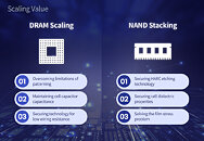
On March 22nd, the CEO of SK Hynix, Seok-Hee Lee, gave a keynote speech to the IEEE International Reliability Physics Symposium (IRPS) and shared with experts a part of its plan for the future of SK Hynix products. The CEO took the stage and delivered some conceptual technologies that the company is working on right now. At the center of the show, two distinct products stood out - 3D NAND and DRAM. So far, the company has believed that its 3D NAND scaling was very limited and that it can push up to 500 layers sometime in the future before the limit is reached. However, according to the latest research, SK Hynix will be able to produce 600-layer 3D NAND technology in the distant future.

So far, the company has managed to manufacture and sample 512Gb 176-layer 3D NAND chips, so the 600-layer solutions are still far away. Nonetheless, it is a possibility that we are looking at. Before we reach that layer number, there are various problems needed to be solved so the technology can work. According to SK Hynix, "the company introduced the atomic layer deposition (ALD) technology to further improve the cell property of efficiently storing electric charges and exporting them when needed, while developing technology to maintain uniform electric charges over a certain amount through the innovation of dielectric materials. In addition to this, to solve film stress issues, the mechanical stress levels of films is controlled and the cell oxide-nitride (ON) material is being optimized. To deal with the interference phenomenon between cells and charge loss that occur when more cells are stacked at a limited height, SK Hynix developed the isolated-charge trap nitride (isolated-CTN) structure to enhance reliability."

AMD's Next-Generation Van Gogh APU Shows Up with Quad-Channel DDR5 Memory Support

AMD is slowly preparing to launch its next-generation client-oriented accelerated processing unit (APU), which is AMD's way of denoting a CPU+GPU combination. The future design is codenamed after Van Gogh, showing AMD's continuous use of historic names for their products. The APU is believed to be a design similar to the one found in the SoC of the latest PlayStation 5 and Xbox Series X/S consoles. That means that there are Zen 2 cores present along with the latest RDNA 2 graphics, side by side in the same processor. Today, one of AMD's engineers posted a boot log of the quad-core Van Gogh APU engineering sample, showing some very interesting information.

The boot log contains information about the memory type used in the APU. In the logs, we see a part that says "[drm] RAM width 256bits DDR5", which means that the APU has an interface for the DDR5 memory and it is 256-bit wide, which represents a quad-channel memory configuration. Such a wide memory bus is typically used for applications that need lots of bandwidth. Given that Van Gogh uses RDNA 2 graphics, the company needs a sufficient memory bandwidth to keep the GPU from starving for data. While we don't have much more information about it, we can expect to hear greater details soon.

Apple is Discontinuing Intel-based iMac Pro

According to the official company website, Apple will no longer manufacture its iMac Pro computers based on Intel processors. Instead, the company will carry these models in its store, only while the supplies last. Apple will be replacing these models with next-generation iMac Pro devices that will be home to the custom Apple Silicon processors, combining Arm CPU cores with custom GPU design. Having a starting price of 4990 USD, the Apple iMac Pro was able to max out at 15000 USD. The most expensive part was exactly the Intel Xeon processor inside it, among the AMD GPU with HBM. Configuration pricing was also driven by storage/RAM options. However, even the most expensive iMac Pro with its 2017 hardware had no chance against the regular 2020 iMac, so the product was set to be discontinued sooner or later.

When the stock of the iMac Pro runs out, Apple will replace this model with its Apple Silicon equipped variant. According to the current rumor mill, Apple is set to hold a keynote on March 16th that will be an announcement for new iMac Pro devices with custom processors. What happens is only up to Apple, so we have to wait and see.

Micron Launches Low-Power Memory Qualified for Automotive Safety Applications

Micron Technology, Inc. today announced that it has begun sampling the industry's first automotive low-power DDR5 DRAM (LPDDR5) memory that is hardware-evaluated to meet the most stringent Automotive Safety Integrity Level (ASIL), ASIL D. The solution is part of Micron's new portfolio of memory and storage products targeted for automotive functional safety based on the International Organization for Standardization (ISO) 26262 standard.

Micron's functional safety-evaluated DRAM is compatible with advanced-driver assistance system (ADAS) technologies, including adaptive cruise control, automatic emergency braking systems, lane departure warning and blind spot detection systems. Micron's LPDDR5's high performance, superior power efficiency and low latency provide the requisite performance and headroom to keep pace with increasing bandwidth requirements of next-generation automotive systems.

"Autonomous vehicles promise to make our roads safer, but they need powerful, trusted memory that can enable real-time decision-making in extreme environments," said Kris Baxter, corporate vice president and general manager of Micron's Embedded Business Unit. "To fulfill this growing market need, we've optimized our automotive LPDDR5 to deliver the utmost performance, quality and reliability for the smart, safe cars of tomorrow."

AMD "Zen 4" Microarchitecture to Support AVX-512

The next-generation "Zen 4" CPU microarchitecture powering AMD's 4th Gen EPYC "Genoa" enterprise processors, will support 512-bit AVX instruction sets, according to an alleged company slide leaked to the web on the ChipHell forums. The slide references "AVX3-512" support in addition to BFloat16 and "other ISA extensions." This would make "Zen 4" the first AMD microarchitecture to support AVX-512. It remains to be seen which specific instructions the architecture supports, and whether all of them are available to both the enterprise and client implementations of "Zen 4," or whether AMD would take an approach similar to Intel, in only enabling certain "relevant" instructions on the client parts. The slide also mentions core counts being "greater than 64" corresponding withour story from earlier today.

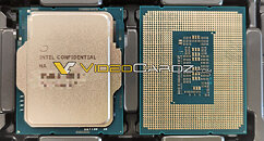
Intel Alder Lake Processor Tested, Big Cores Ramp Up to 3 GHz

Intel "Alder Lake" is the first processor generation coming from the company to feature the hybrid big.LITTLE type core arrangement and we are wondering how the configurations look like and just how powerful the next-generation processors are going to be. Today, a Geekbench submission has appeared that gave us a little more information about one out of twelve Alder Lake-S configurations. This time, we are getting an 8-core, 16-threaded design with all big cores and no smaller cores present. Such design with no little cores in place is exclusive to the Alder Lake-S desktop platform, and will not come to the Alder Lake-P processors designed for mobile platforms.

Based on the socket LGA1700, the processor was spotted running all of its eight cores at 2.99 GHz frequency. Please note that this is only an engineering sample and the clock speeds of the final product should be higher. It was paired with the latest DDR5 memory and NVIDIA GeForce RTX 2080 GPU. The OpenCL score this CPU ran has shown that it has provided the GPU with more than enough performance. Typically, the RTX 2080 GPU scores about 106101 points in Geekbench OpenCL tests. Paired with the Alder Lake-S CPU, the GPU has managed to score as much as 108068 points, showing the power of the new generation of cores. While there is still a lot of mystery surrounding the Alder Lake-S series, we have come to know that the big cores used are supposed to be very powerful.
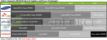
Explosive Growth in Automotive DRAM Demand Projected to Surpass 30% CAGR in Next Three Years, Says TrendForce

Driven by such factors as the continued development of autonomous driving technologies and the build-out of 5G infrastructure, the demand for automotive memories will undergo a rapid growth going forward, according to TrendForce's latest investigations. Take Tesla, which is the automotive industry leader in the application of autonomous vehicle technologies, as an example. Tesla has adopted GDDR5 DRAM products from the Model S and X onward because it has also adopted Nvidia's solutions for CPU and GPU. The GDDR5 series had the highest bandwidth at the time to complement these processors. The DRAM content has therefore reached at least 8 GB for vehicles across all model series under Tesla. The Model 3 is further equipped with 14 GB of DRAM, and the next-generation of Tesla vehicles will have 20 GB. If content per box is used as a reference for comparison, then Tesla far surpasses manufacturers of PCs and smartphones in DRAM consumption. TrendForce forecasts that the average DRAM content of cars will continue to grow in the next three years, with a CAGR of more than 30% for the period.

AMD Ryzen 7 Pro 5750G Zen 3 Based Desktop APU Spotted with 4.75 GHz Frequency

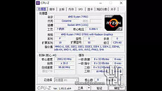
AMD is slowly preparing the launch of its next-generation Ryzen Pro 5000 series of APUs designed for desktop applications. The biggest difference over the previous generation Renoir 4000 series is that this generation is now offering a major improvement in microarchitecture. Using Zen 3 core at its base, the Cezanne processor lineup is supposed to integrate all of the IPC improvements and bring them to the world of APUs. Doubling the level three (L3) cache capacity from 8 MB to 16 MB, Zen 3 cores are paired with a good amount of cache to improve performance.

Thanks to a user from Chiphell forums, we have the first details about AMD Ryzen 7 Pro 5750G APU. The new generation design is bringing a big improvement with clock speeds. Having a base frequency of 3.8 GHz, the Zen 3 based design now goes up to 4.75 GHz, representing a 350 MHz increase over the past generation Ryzen 7 Pro 4750G APU. For more details, we have to wait for the official announcement.
AMD Ryzen 7 Pro 5750G AMD Cezanne

AMD Talks Zen 4 and RDNA 3, Promises to Offer Extremely Competitive Products

AMD is always in development mode and just when they launch a new product, the company is always gearing up for the next-generation of devices. Just a few months ago, back in November, AMD has launched its Zen 3 core, and today we get to hear about the next steps that the company is taking to stay competitive and grow its product portfolio. In the AnandTech interview with Dr. Lisa Su, and The Street interview with Rick Bergman, the EVP of AMD's Computing and Graphics Business Group, we have gathered information about AMD's plans for Zen 4 core development and RDNA 3 performance target.

Starting with Zen 4, AMD plans to migrate to the AM5 platform, bringing the new DDR5 and USB 4.0 protocols. The current aim of Zen 4 is to be extremely competitive among competing products and to bring many IPC improvements. Just like Zen 3 used many small advances in cache structures, branch prediction, and pipelines, Zen 4 is aiming to achieve a similar thing with its debut. The state of x86 architecture offers little room for improvement, however, when the advancement is done in many places it adds up quite well, as we could see with 19% IPC improvement of Zen 3 over the previous generation Zen 2 core. As the new core will use TSMC's advanced 5 nm process, there is a possibility to have even more cores found inside CCX/CCD complexes. We are expecting to see Zen 4 sometime close to the end of 2021.

Intel CEO Says Using Competitor's Semiconductor Process in Intel Fabs is an Option

Semiconductor manufacturing is not an easy feat to achieve. Especially if you are constantly chasing the smaller and smaller node. Intel knows this the best. The company has had a smooth transition from other nodes to the smaller ones until the 10 nm node came up. It has brought Intel years of additional delay and tons of cost improving the yields of a node that was seeming broken. Yesterday the company announced the new Tiger Lake-H processors for laptops that are built using the 10 nm process, however, we are questioning whatever Intel can keep up with the semiconductor industry and deliver the newest nodes on time, and with ease. During an interview with Intel's CEO Bob Swan, we can get a glimpse of Intel's plans for the future of semiconductors at the company.

In the interview, Mr. Swan has spoken about the technical side of Intel and how the company plans to utilize its Fabs. The first question everyone was wondering was about the state of 10 nm. The node is doing well as three Fabs are ramping up capacity every day, and more products are expected to arrive on that node. Mr. Swan has also talked about outsourcing chip production, to which he responded by outlining the advantage Intel has with its Fabs. He said that outsourcing is what is giving us shortages like AMD and NVIDIA experience, and Intel had much less problems. Additionally, Mr. Swan was asked about the feasibility of new node development. To that, he responded that there is a possibility that Intel could license its competitor's node and produce it in their Fabs.

Intel Confirms HBM is Supported on Sapphire Rapids Xeons

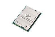
Intel has just released its "Architecture Instruction Set Extensions and Future Features Programming Reference" manual, which serves the purpose of providing the developers' information about Intel's upcoming hardware additions which developers can utilize later on. Today, thanks to the @InstLatX64 on Twitter we have information that Intel is bringing on-package High Bandwidth Memory (HBM) solution to its next-generation Sapphire Rapids Xeon processors. Specifically, there are two instructions mentioned: 0220H - HBM command/address parity error and 0221H - HBM data parity error. Both instructions are there to address data errors in HBM so the CPU operates with correct data.

The addition of HBM is just one of the many new technologies Sapphire Rapids brings. The platform is supposedly going to bring many new technologies like an eight-channel DDR5 memory controller enriched with Intel's Data Streaming Accelerator (DSA). To connect to all of the external accelerators, the platform uses PCIe 5.0 protocol paired with CXL 1.1 standard to enable cache coherency in the system. And as a reminder, this would not be the first time we see a server CPU use HBM. Fujitsu has developed an A64FX processor with 48 cores and HBM memory, and it is powering today's most powerful supercomputer - Fugaku. That is showing how much can a processor get improved by adding a faster memory on-board. We are waiting to see how Intel manages to play it out and what we end up seeing on the market when Sapphire Rapids is delivered.

AMD Ryzen 5 5600H "Cezanne" Processor Benchmarked, Crushes Renoir in Single Core and Multi Core Performance

With the launch of AMD's next-generation mobile processors just around the corner, with an expected launch date in the beginning of 2021 at the CES virtual event. The Cezanne lineup, as it is called, is based on AMD's latest Zen 3 core, which brings many IPC improvements, along with better frequency scaling thanks to the refined architecture design. Today, we get to see just how much the new Cezanne generation brings to the table thanks to the GeekBench 5 submission. In the test system, a Ryzen 5 5600H mobile processor was used, found inside of a Xiaomi Mi Notebook, paired with 16 GB of RAM.

As a reminder, the AMD Ryzen 5 5600H is a six-core, twelve threaded processor. So you are wondering how the performance looks like. Well, in the single-core test, the Zen 3 enabled core has scored 1372 points, while the multi-threaded performance result equaled 5713 points. If we compare that to the last generation Zen 2 based "Renoir" design, the equivalent Ryzen 5 4600H processor, the new design is about 37% faster in single-threaded, and about 14% faster in multi-threaded workloads. We are waiting for the announcement to see the complete AMD Cezanne lineup and see the designs it will bring.

NVIDIA to Introduce an Architecture Named After Ada Lovelace, Hopper Delayed?

NVIDIA has launched its GeForce RTX 3000 series of graphics cards based on the Ampere architecture three months ago. However, we are already getting information about the next-generation that the company plans to introduce. In the past, the rumors made us believe that the architecture coming after Ampere is allegedly being called Hopper. Hopper architecture is supposed to bring multi-chip packaging technology and be introduced after Ampere. However, thanks to @kopite7kimi on Twitter, a reliable source of information, we have data that NVIDIA is reportedly working on a monolithic GPU architecture that the company internally refers to as "ADxxx" for its codenames.

The new monolithically-designed Lovelace architecture is going make a debut on the 5 nm semiconductor manufacturing process, a whole year earlier than Hopper. It is unknown which foundry will manufacture the GPUs, however, both of NVIDIA's partners, TSMC and Samsung, are capable of manufacturing it. The Hopper is expected to arrive sometime in 2023-2024 and utilize the MCM technology, while the Lovelace architecture will appear in 2021-2022. We are not sure if the Hopper architecture will be exclusive to data centers or extend to the gaming segment as well. The Ada Lovelace architecture is supposedly going to be a gaming GPU family. Ada Lovelace, a British mathematician, has appeared on NVIDIA's 2018 GTC t-shirt known as "Company of Heroes", so NVIDIA may have already been using the ADxxx codenames internally for a long time now.

128-Core 2P AMD EPYC "Milan" System Benchmarked in Cinebench R23, Outputs Insane Numbers

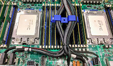
AMD is preparing to launch its next-generation of EPYC processors codenamed Millan. Being based on the company's latest Zen 3 cores, the new EPYC generation is going to deliver a massive IPC boost, spread across many cores. Models are supposed to range anywhere from 16 to 64 cores, to satisfy all of the demanding server workloads. Today, thanks to the leak from ExecutableFix on Twitter, we have the first benchmark of a system containing two of the 64 core, 128 thread Zen 3 based EPYC Milan processors. Running in the 2P configuration the processors achieved a maximum boost clock of 3.7 GHz, which is very high for a server CPU with that many cores.

The system was able to produce a Cinebench R23 score of insane 87878 points. With that many cores, it is no wonder how it is done, however, we need to look at how does it fare against the competition. For comparison, the Intel Xeon Platinum 8280L processor with its 28 cores and 56 threads that boost to 4.0 GHz can score up to 49,876 points. Of course, the scaling to that many cores may not work very well in this example application, so we have to wait and see how it performs in other workloads before jumping to any conclusions. The launch date is unknown for these processors, so we have to wait and report as more information appears.

AMD CEO Dr. Lisa Su to Present at CES 2021 Virtual Keynote

AMD has just had quite an amazing year. From the launch of the Ryzen 5000 series CPUs based on Zen 3 architecture to RDNA 2 based graphics cards, the company has been delivering new solutions in a timely manner. With the upcoming tech conference being CES, we are wondering which companies are going to hold their keynotes virtually. Thanks to the official CES website, we have confirmation that AMD's CEO Dr. Lisa Su will hold a virtual keynote with the goal of "presenting the AMD vision for the future of research, education, work, entertainment, and gaming, including a portfolio of high-performance computing and graphics solutions." That could mean that we could possibly see some new directions for the company and how AMD plans to develop next-generation computing solutions, so stay tuned for more interesting information coming your way on January 11th, when CES kicks-off.

TSMC Completes Its Latest 3 nm Factory, Mass Production in 2022

They say that it is hard to keep up with Moore's Law, however, for the folks over at Taiwan Semiconductor Manufacturing Company (TSMC), that doesn't seem to represent any kind of a problem. Today, to confirm that TSMC is one of the last warriors for the life of Moore's Law, we have information that the company has completed building its manufacturing facility for the next-generation 3 nm semiconductor node. Located in Southern Taiwan Science Park near Tainan, TSMC is expecting to start high-volume manufacturing of the 3 nm node in that Fab in the second half of 2022. As always, one of the first customers expected is Apple.

Estimated to cost an amazing 19.5 billion US Dollars, the Fab is expected to have an output of 55,000 300 mm (12-inch) wafers per month. Given that the regular facilities of TSMC exceed the capacity of over 100K wafers per month, this new facility is expected to increase the capacity over time and possibly reach the 100K level. The new 3 nm node is going to use the FinFET technology and will deliver a 15% performance gain over the previous 5 nm node, with 30% decreased power use and up to 70% density increase. Of course, all of those factors will depend on a specific design.

BittWare Launches IA-840F with Intel Agilex FPGA and Support for oneAPI

BittWare, a Molex company, today unveiled the IA-840F, the company's first Intel Agilex -based FPGA card designed to deliver significant performance-per-watt improvements for next-generation data center, networking and edge compute workloads. Agilex FPGAs deliver up to 40% higher performance or up to 40% lower power, depending on application requirements. BittWare maximized I/O features using the Agilex chip's unique tiling architecture with dual QSFP-DDs (4× 100G), PCIe Gen4 x16, and three MCIO expansion ports for diverse applications. BittWare also announced support for Intel oneAPI, which enables an abstracted development flow for dramatically simplified code re-use across multiple architectures.

"Modern data center workloads are incredibly diverse, requiring customers to implement a mix of scalar, vector, matrix and spatial architectures," said Craig Petrie, vice president of marketing for BittWare. "The IA-840F ensures that customers can quickly and easily exploit the advanced features of the Intel Agilex FPGA. For those customers who prefer to develop FPGA applications at an abstracted level, we are including support for oneAPI. This new unified software programming environment allows customers to program the Agilex FPGA from a single code base with native high-level language performance across architectures."

NVIDIA Announces Mellanox InfiniBand for Exascale AI Supercomputing

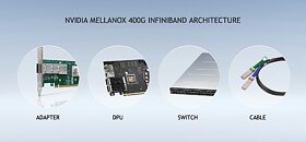
NVIDIA today introduced the next generation of NVIDIA Mellanox 400G InfiniBand, giving AI developers and scientific researchers the fastest networking performance available to take on the world's most challenging problems.

As computing requirements continue to grow exponentially in areas such as drug discovery, climate research and genomics, NVIDIA Mellanox 400G InfiniBand is accelerating this work through a dramatic leap in performance offered on the world's only fully offloadable, in-network computing platform. The seventh generation of Mellanox InfiniBand provides ultra-low latency and doubles data throughput with NDR 400 Gb/s and adds new NVIDIA In-Network Computing engines to provide additional acceleration.

AMD Looks to Keep Performance, Efficiency Gains Momentum With Zen 4, RDNA 3, and Commitment to Threadripper

AMD's Executive Vice President Rick Bergman in an interview with The Street shed some light on the company's future plans for Zen 4 and RDNA 3, even as we are still reeling from (or coming in to) Zen 3 and RDNA 2's launches. Speaking on RDNA 3, Rick Bergman mentioned the company's commitment to achieve the same 50% performance-per-watt increase they achieved with RDNA 2, and had some interesting takes on the matter of why this is actually one of the most important metrics:
Rick BergmanIt just matters so much in many ways, because if your power is too high -- as we've seen from our competitors -- suddenly our potential users have to buy bigger power supplies, very advanced cooling solutions. And in a lot of ways, very importantly, it actually drives the [bill of materials] of the board up substantially. This is a desktop perspective. And invariably, that either means the retail price comes up, or your GPU cost has to come down. We focused on that for RDNA 2. It's a big focus on RDNA 3 as well.

AMD Radeon RX 6800 and RX 6800 XT GPU OpenCL Performance Leaks

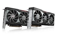
AMD has just recently announced its next-generation Radeon RX 6000 series GPU based on the new RDNA 2 architecture. The architecture is set to compete with NVIDIA Ampere architecture and highest offerings of the competing company. Today, thanks to the well-known leaker TUM_APISAK, we have some Geekbench OpenCL scores. It appears that some user has gotten access to the system with the Radeon RX 6800 and RX 6800 XT GPUs, running Cinebench 4.4 OpenCL tests. In the tests, the system ran on the Intel platform with Core i9-10900K CPU with 16 GB DDR4 RAM running at 3600 MHz. The motherboard used was ASUS top-end ROG Maximus XII Extreme Z490 board.

When it comes to results, the system with RX 6800 GPU scored anywhere from 347137 points to 336367 points in three test runs. For comparison, NVIDIA GeForce RTX 3070 scores about 361042 points, showcasing that the Radeon card is not faster in any of the runs. When it comes to the higher-end Radeon RX 6800 XT GPU, it scored 407387 and 413121 points in two test runs. Comparing that to GeForce RTX 3080 GPU that scores 470743 points, the card is slower compared to the competition. There has been a Ryzen 9 5950X test setup that boosted the performance of Radeon RX 6800 XT card by quite a lot, making it reach 456837 points, making a huge leap over the Intel-based system thanks to the Smart Access Memory (SAM) technology that all-AMD system provides.
Return to Keyword Browsing
May 16th, 2024 16:52 EDT change timezone

New Forum Posts

Popular Reviews

Controversial News Posts