Tuesday, March 23rd 2021

SK Hynix Envisions the Future: 600-Layer 3D NAND and EUV-made DRAM
On March 22nd, the CEO of SK Hynix, Seok-Hee Lee, gave a keynote speech to the IEEE International Reliability Physics Symposium (IRPS) and shared with experts a part of its plan for the future of SK Hynix products. The CEO took the stage and delivered some conceptual technologies that the company is working on right now. At the center of the show, two distinct products stood out - 3D NAND and DRAM. So far, the company has believed that its 3D NAND scaling was very limited and that it can push up to 500 layers sometime in the future before the limit is reached. However, according to the latest research, SK Hynix will be able to produce 600-layer 3D NAND technology in the distant future.
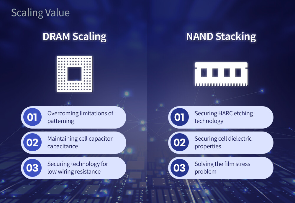
So far, the company has managed to manufacture and sample 512Gb 176-layer 3D NAND chips, so the 600-layer solutions are still far away. Nonetheless, it is a possibility that we are looking at. Before we reach that layer number, there are various problems needed to be solved so the technology can work. According to SK Hynix, "the company introduced the atomic layer deposition (ALD) technology to further improve the cell property of efficiently storing electric charges and exporting them when needed, while developing technology to maintain uniform electric charges over a certain amount through the innovation of dielectric materials. In addition to this, to solve film stress issues, the mechanical stress levels of films is controlled and the cell oxide-nitride (ON) material is being optimized. To deal with the interference phenomenon between cells and charge loss that occur when more cells are stacked at a limited height, SK Hynix developed the isolated-charge trap nitride (isolated-CTN) structure to enhance reliability."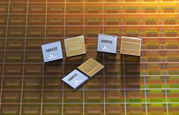
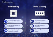 When it comes to DRAM, the company is looking to overcome some very interesting problems. By using extreme ultraviolet (EUV) lithography, the company can solve the limitation of patterning on non-EUV processes. Things are looking very bright and the process should get below 10 nm easily. To keep the cell capacitance in check, SK Hynix is trying to refine the dielectric thickness and develop new materials with high dielectric constant. All of those capacitive cells need to interconnect, and to get as low resistance as possible, the company is working on the next-generation electrode and insulating materials.
However, this is not everything that the South Korean company has to work on. The CEO talked about the convergence of memory and logic, with the current industry trend being just that. So far, we have seen processing near memory, like we see with chips with HBM stacked just next to it; processing in memory, where the processor is present with memory in a single package. But, SK Hynix wants to use a new approach of computing in-memory concept, where the memory is capable of performing computation by itself. Applications such as AI and machine learning would benefit the most, along with other uses we think of in the meantime. What we will end up with is not known, as the company only showcased a concept, so the final products are still a few years away.
Source:
SK Hynix
So far, the company has managed to manufacture and sample 512Gb 176-layer 3D NAND chips, so the 600-layer solutions are still far away. Nonetheless, it is a possibility that we are looking at. Before we reach that layer number, there are various problems needed to be solved so the technology can work. According to SK Hynix, "the company introduced the atomic layer deposition (ALD) technology to further improve the cell property of efficiently storing electric charges and exporting them when needed, while developing technology to maintain uniform electric charges over a certain amount through the innovation of dielectric materials. In addition to this, to solve film stress issues, the mechanical stress levels of films is controlled and the cell oxide-nitride (ON) material is being optimized. To deal with the interference phenomenon between cells and charge loss that occur when more cells are stacked at a limited height, SK Hynix developed the isolated-charge trap nitride (isolated-CTN) structure to enhance reliability."

However, this is not everything that the South Korean company has to work on. The CEO talked about the convergence of memory and logic, with the current industry trend being just that. So far, we have seen processing near memory, like we see with chips with HBM stacked just next to it; processing in memory, where the processor is present with memory in a single package. But, SK Hynix wants to use a new approach of computing in-memory concept, where the memory is capable of performing computation by itself. Applications such as AI and machine learning would benefit the most, along with other uses we think of in the meantime. What we will end up with is not known, as the company only showcased a concept, so the final products are still a few years away.
13 Comments on SK Hynix Envisions the Future: 600-Layer 3D NAND and EUV-made DRAM
I worked at a place that hammered all the walls with they're patents, as a kind of art,. I loved it, great read but I sware they're was an Aire of comedy to it too.
Like ,
patent A a pipe
Patent B a pipe In a pipe(not pipe could be banana)
Patent C a pipe in a pipe in a pipe ( not necessarily a pipe, could be a banana)
All with diagrams.
(The dies are usually stacked, that's obvious, but I mean layers similar to those in NAND.)
-a smooth curve
-a smooth curve with a radius on it
-a smooth curve with a radius on a radius on it ;)
www.bbc.com/future/article/20191108-why-the-world-is-running-out-of-sand
but again, i know that must be impossible, as I have no idea how it all works. otherwise someone would have done it by now.
Silicon is a substrate it cant just keep getting better intel and and nvidea are already dam well pushing that performance wall
eventually it will be fully impossible to get any more performance out a silicon chip and then we need a replacement