Monday, March 5th 2012

GK104 Die-Size Estimated

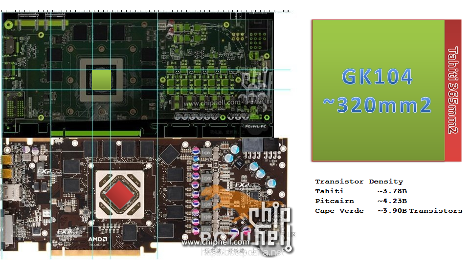
Thanks to some good understanding of geometry, and great Photoshop skills, the punters have estimated the die-size of NVIDIA's GeForce Kepler 104 (GK104) GPU, using a picture of the NVIDIA reference board that was leaked last week. Compared to the known die-size of an AMD "Tahiti"-based graphics card, the die-size of GK104 was estimated to be around 320 mm², about 45 mm² smaller than Tahiti. The relative transistor density of the chip, compared to AMD's 28 nm chips, were also estimated.
Source: XtremeSystems Forums
Add your own comment

27 Comments on GK104 Die-Size Estimated

#1
seronx
If it is priced around $299 it follows the usual mm² = price.
Posted on Reply
#2
MxPhenom 216
ASIC Engineer
so much for nvidia's reputation of building massive dies.
Posted on Reply
#3
phanbuey
They are definitely doing something out of the norm.
Posted on Reply
#4
arnoo1
i hope this is true, then we are finally going to see some small die'sfrom nvidia, i hope this means lower power consumption and alot of transitors i hope gtx 670ti/gtx680 is going to be a killer chip
Posted on Reply
#5
Crap Daddy
There's no reason why it shouldn't.
Posted on Reply
#6
GSquadron
I dont get it why amd puts the chip in 45degree rotation and nvidia doesnt?
Posted on Reply
#7
dj-electric
It's just the optimal way for the wiring inside the PCB to the rest of the components involved.
Posted on Reply
#8
Casecutter
What we need to know to truly understand Nvidia price per wafer advantage is what the 570/580 Dia. (520mm²) so this should mean Nvidia has 37% increase in chips. Although factor that 28Nm wafer is probably seeing a 20-25% in increase in cost to each chip, so they might cost less I would think like 15%. So if a GTX570 MSRP was $475 we should see a similar 28Nm for $400. I can’t see Nvidia selling better then GTX570 performance for 35% under the perf/$ and lose money per chip. I just don’t see the sweet spot of what a wafer providing going for $300. Sure cut-back/ geldings might be (GTX570) $300, the norm of binning is $350-380, while top shelf 7970 busters at $420. If Nvidia can deliver a bulk of chip that unseat a 7970 at that price it would will have a big impact. The average cost of card from GK104 silicon providing say a $330 average as a family when all it said and done.

Cayman had a 389mm² vs. Tahiti XT 378mm² that 1-2% improvement, so any 28Nm wafer price inflicted by TSMC was almost a fully impacted to the end user.
So yes Nvidia curtailing the dia for this go-around was a great move Now If Nvidia does pass that saving to those purchasing that would be another bold move, and very uncharacteristic of what they’ve done in the past.

Though be careful what you wish for what if AMD has Global Foundries doing their production next round and TMSC has less 28Nm production so they’re compelled to raise Nvidia’s next re-spin price to keep their shareholders happy. Did TSMC tell Nvidia even earlier that price would increase giving Nvidia an unfair advantage to start shrink the Fermi 2 years ago?
Posted on Reply
#9
phanbuey
They need to release these already. Im ready for the 760Ti.
Posted on Reply
#10
Benetanegia
btarunrThe relative transistor density of the chip, compared to AMD's 28 nm chips, were also estimated.
Unless I'm mistaken aren't those numbers representing the posible amount of transistors on GK104 if transistor density was that of Tahiti, Pitcairn or CV?
Posted on Reply
#11
OneCool
omg!!

This is getting out of control :rolleyes:
Posted on Reply
#12
D4S4
:twitch:

what, nvidia having a smaller die size than ati?! the world really is coming to an end this year. :laugh:
Posted on Reply
#13
Benetanegia
D4S4:twitch:

what, nvidia having a smaller die size than ati?! the world really is coming to an end this year. :laugh:
It wouldn't be the first time. G71 was 2/3rds the size of R580.

I'm not really telling this to you, but if someone wants to talk about that issue seriously, people should really look past the old misconceptions, because Nvidia has been making bigger chips not because of an inherent disadvantage, but because of a reason: compute. Now AMD is going after compute too and their die size is much bigger than you would have expected in the past from a similar performing card in a new process. Nvidia has never really been too far behind AMD in perf/area, but it's just something that needs to be seen with some perspective, and most people just don't.

Take GT200 for example, one of the worst in that respect. It was freaking huge, but it was made in 65 nm instead of in 55nm and the most important thing is that it had 30 double precision processors on top of the 240 single precision ones, that could only be accesed by CUDA (no gaming). DP shaders are at least twice as big as single precision ones, so had Nvidia focused on gaming, GT200 would have been a 300 SP gaming chip. That's a 25% increase! Imagine GTX285 being 25% faster, that's as fast as HD5870 and now compare that to HD4870 and evaluate perf/area again on 55nm (260 vs 480 mm^2). It's a completely different story isn't it?
Posted on Reply
#14
BrooksyX
I feel like Nvidia is just trying way to hard to create buzz around the kepler because they know the AMD 7xxx is doing pretty good. They just need to release the card so we can see if the can put their money where their mouth is!

However I personally I am perfectly happy with my 6870 and will probably skip this generation.
Posted on Reply
#15
cc101385
they better be good.

7870's power efficiency is pretty impressive. about as powerful as gtx580 but consumes half of the power draw.
Posted on Reply
#16
Aquinus
Resident Wat-man
I want nVidia to release something already. :cry:
Posted on Reply
#17
phanbuey
BrooksyXI feel like Nvidia is just trying way to hard to create buzz around the kepler because they know the AMD 7xxx is doing pretty good. They just need to release the card so we can see if the can put their money where their mouth is!

However I personally I am perfectly happy with my 6870 and will probably skip this generation.
I feel like that is something that is true because of the pricing as well. The 7xxx series has moved pricing up so high that it makes it hard to get excited about...

I mean - i can spend the same amount of money that I spent close to a year ago... to replace my card with a card that costs about the same and performs about the same with lower power consumption without any new tech... Thats like buying a new card for the sake of buying a new card. Meh.
Posted on Reply
#18
Sapientwolf
BenetanegiaUnless I'm mistaken aren't those numbers representing the posible amount of transistors on GK104 if transistor density was that of Tahiti, Pitcairn or CV?
I agree, that statement is phrased erroneously. It should say "The total transistor count is estimated based on the transistor densities of Tahiti, Pitcairn and Cape Verde."

Which also means the diagram is labeled wrong as well. Transistor density should be Transistors/mm^2.

Total transistor count should be Transistor Density * Die Area = Estimated Transistor Count.
Posted on Reply
#19
EarthDog
Ok, who here has Die envy, raise your hands...
Posted on Reply
#20
Over_Lord
News Editor
A 212mm^2 so called HD7870 GPU by AMD beat HD7970(362mm^2 I believe) GPU when overclocked around 18% (achieved with stock cooler itself).
Posted on Reply
#21
xenocide
thunderisingA 212mm^2 so called HD7870 GPU by AMD beat HD7970(362mm^2 I believe) GPU when overclocked around 18% (achieved with stock cooler itself).
If you're pulling that from the TPU review, I don't know how much stock I'd put into that. According to that the 6970 is better than the 7950. 1 benchmark never tells the whole story.
Posted on Reply
#22
THE_EGG
hmm from what I see in that picture, looks like there will be the 6pin + 8pin stack (which we saw earlier) and it looks like there are solder points for another 6 pin. :/ why not just 2X 8 pins :/ Hopefully this allows the addition (by the user/consumer) of another 6 pin connector like with some of the 8xxx and 9xxx cards by Nvidia.
Posted on Reply
#23
NHKS
typo?
phanbueyThey need to release these already. Im ready for the 760Ti.
I hope u mean 670Ti. :)
I understand, its easy to get carried away with lots of leaks and speculation around the GK104.
Posted on Reply
#24
Aquinus
Resident Wat-man
NHKSI hope u mean 670Ti. :)
I understand, its easy to get carried away with lots of leaks and speculation around the GK104.
It's running rampent. :)
Posted on Reply
#25
D4S4
BenetanegiaIt wouldn't be the first time. G71 was 2/3rds the size of R580.

I'm not really telling this to you, but if someone wants to talk about that issue seriously, people should really look past the old misconceptions, because Nvidia has been making bigger chips not because of an inherent disadvantage, but because of a reason: compute. Now AMD is going after compute too and their die size is much bigger than you would have expected in the past from a similar performing card in a new process. Nvidia has never really been too far behind AMD in perf/area, but it's just something that needs to be seen with some perspective, and most people just don't.

Take GT200 for example, one of the worst in that respect. It was freaking huge, but it was made in 65 nm instead of in 55nm and the most important thing is that it had 30 double precision processors on top of the 240 single precision ones, that could only be accesed by CUDA (no gaming). DP shaders are at least twice as big as single precision ones, so had Nvidia focused on gaming, GT200 would have been a 300 SP gaming chip. That's a 25% increase! Imagine GTX285 being 25% faster, that's as fast as HD5870 and now compare that to HD4870 and evaluate perf/area again on 55nm (260 vs 480 mm^2). It's a completely different story isn't it?
dude, i was kidding.
Posted on Reply
Add your own comment
Apr 25th, 2024 00:37 EDT change timezone

New Forum Posts

Popular Reviews

Controversial News Posts