Thursday, February 6th 2014

NVIDIA GM107 "Maxwell" Silicon Pictured
Here is the first picture of a couple of NVIDIA GM107 silicons in a tray, ahead of graphics card assembly. The packages appear to be as big as those of the GK106 from the previous generation, however, the die itself is estimated to be smaller, at roughly 156 mm², compared to the 221 mm² die of the GK106, and the 118 mm² of the GK107. The best part? All three chips are built on the same 28 nm silicon fab process. So what makes the GM107 die smaller than that of the GK106 despite having a similar feature-set? Narrower memory bus. The GM107 is said to feature a 128-bit wide GDDR5 memory interface, in comparison to the 192-bit wide interface of the GK106.
Apart from the 128-bit wide GDDR5 memory interface, the GM107 is said to feature a total of 960 CUDA cores, 80 TMUs, and 16 ROPs. The CUDA core count is identical to that of the GK106. The GM107 is built on NVIDIA's next-generation "Maxwell" GPU architecture. It will form the foundation of two SKUs, the GeForce GTX 750 Ti, and the GeForce GTX 750. The former features the full complement of 960 CUDA cores; while the latter is slightly cut down, and features just 768. The TDP of the GTX 750 Ti is approximated to be around 75 Watt. If true, the GTX 750 duo will set new standards on the performance-per-Watt metrics. NVIDIA is expected to launch both, later this month.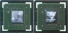
Source:
VideoCardz
Apart from the 128-bit wide GDDR5 memory interface, the GM107 is said to feature a total of 960 CUDA cores, 80 TMUs, and 16 ROPs. The CUDA core count is identical to that of the GK106. The GM107 is built on NVIDIA's next-generation "Maxwell" GPU architecture. It will form the foundation of two SKUs, the GeForce GTX 750 Ti, and the GeForce GTX 750. The former features the full complement of 960 CUDA cores; while the latter is slightly cut down, and features just 768. The TDP of the GTX 750 Ti is approximated to be around 75 Watt. If true, the GTX 750 duo will set new standards on the performance-per-Watt metrics. NVIDIA is expected to launch both, later this month.

29 Comments on NVIDIA GM107 "Maxwell" Silicon Pictured
650 TI Boost = 768 / 64 / 24
750 Ti = 960 / 80 / 16
R7 260X = 896 / 56 / 16
R7 260X @ $119
R7 260X OC @ $139
GTX 750 @ $119
GTX 750 Ti @ $139-$149
It might be a competitor to the R7 260X after 5months of its release.
Reference PCB shows option for PCI-E 6-pin, but not used in this case