Thursday, March 6th 2014

NVIDIA GeForce GTX 860M Detailed

NVIDIA slipped out the first mobile GPU based on its GM107 silicon, the GeForce GTX 860M, which was spotted on the forumscape. The GTX 860M is configured identically to the desktop GTX 750 Ti, featuring the chip's full complement of 640 CUDA cores, 40 TMUs, 16 ROPs, and a 128-bit wide GDDR5 memory interface, holding 2 GB of memory. The core is clocked at 540 MHz, and the memory at 5.00 GHz (GDDR5 effective).

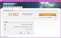
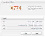
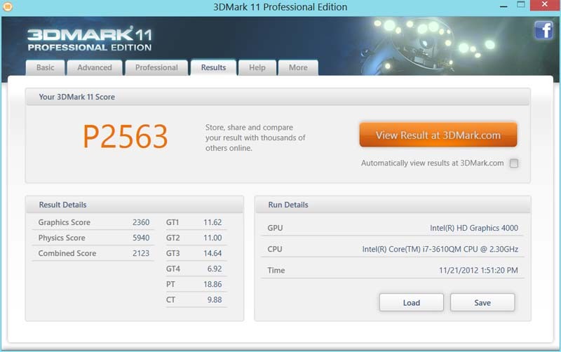
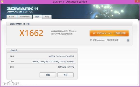
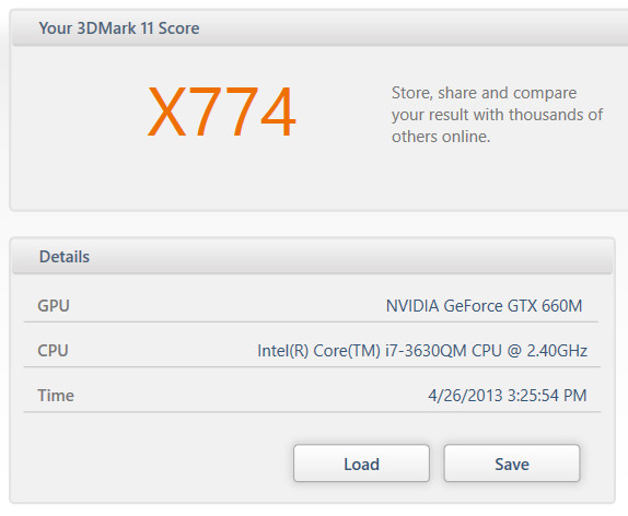
The mobile MXM card was put through a battery of synthetic tests, in which it was found to be twice as fast as its predecessor, the GTX 660M. In 3DMark 11 (performance preset), it scored P5339, compared to the P2563 points scored by the GTX 660M. In 3DMark 11 (extreme preset), the story is similar, with the GTX 860M scoring X1662, compared to the X774 scored by the GTX 660M.
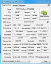
Source: NotebookReview Forums
Add your own comment

20 Comments on NVIDIA GeForce GTX 860M Detailed

#1
megamanxtreme
Ouch! I was so excited when I thought I saw GTX 860, but then I saw the M next to the 0. *Sigh*
Great performance, though.
Posted on Reply
#2
HumanSmoke
I'd really take that 540 MHz core clock with a large grain of salt. The poster at NotebookReview even said as much. The last time Nvidia put out a 500MHz core mobile part it was one very low power (20 watt) GK107 of two years ago- the rest of the recent Nvidia mobile parts are 660-980MHz
Posted on Reply
#3
Prima.Vera
How is this compared to a M7970 or a a M780GTX ?
Posted on Reply
#4
HumanSmoke
Prima.VeraHow is this compared to a M7970 or a a M780GTX ?
Both the 7970M and 780M are 100 watt TDP boards, I wouldn't expect too much from a 45 watt 860M
HD 7970M
GTX 780M
Posted on Reply
#5
carbonytte
HumanSmokeBoth the 7970M and 780M are 100 watt TDP boards, I wouldn't expect too much from a 45 watt 860M
HD 7970M
GTX 780M
I believe the 45W is the onboard version of 860M, the MXM version is 75W, probably that is more comparable to the MXM cards you're trying to compare with.
Posted on Reply
#6
HumanSmoke
carbonytteI believe the 45W is the onboard version of 860M, the MXM version is 75W, probably that is more comparable to the MXM cards you're trying to compare with.
I was under the impression that the MXM 860M had 4GB of vRAM which accounts for a large part of the power increase. The onboard version (the one tested in the article) has 2GB vRAM.
FWIW: I wasn't making any comparison. I just provided a couple of links to the SKUs another poster asked about.
Posted on Reply
#7
dwade
Uggh. It's predecessor is actually the 760m. Not the 2012's 660m.
Posted on Reply
#8
Ali bakhshi
i hope nvidia anounces the GTX 880 soon...i cant wait to see how much TDP dose it have..and the benchmark.
Posted on Reply
#9
carbonytte
@HumanSmoke: Oh sorry. Yeah comparing the cards with the onboard GTX460M, the cards Prima.Vera mentioned should score better.

@Ali bakhshi: 880m ? I previously heard of them but they were Kepler-based, is nVidia releasing Maxwell-based 880m as well?
Posted on Reply
#10
Ali bakhshi
carbonytte@HumanSmoke: Oh sorry. Yeah comparing the cards with the onboard GTX460M, the cards Prima.Vera mentioned should score better.

@Ali bakhshi: 880m ? I previously heard of them but they were Kepler-based, is nVidia releasing Maxwell-based 880m as well?
no i wanna see GTX 880 maxwell soon.for PC not notebook.
Posted on Reply
#12
The Quim Reaper
Lol..strip away the ESRAM and this is just as powerful as the GPU inside the Xbox One.
Posted on Reply
#13
ShockG
Hmmm have a notebook with the 870M here and lots of GPU RAM (4GB+) 3DMark Firestrike is 5.5K~
Seems pretty ok I think
Posted on Reply
#14
haswrong
how much $?
can i solder it to a 2 year old all-in-one pc and expect it to work?
Posted on Reply
#15
HumanSmoke
haswronghow much $?
can i solder it to a 2 year old all-in-one pc and expect it to work?
Of course! You're obviously adept at BGA reballing, so it should be a piss easy task to work out the pinouts of two different GPUs and rewire the socket accordingly.
You don't want to accidentally kill your PC, so I'd suggest a practice run first to get acquainted with the methodology¹:
1. Buy a R9 290X, lever the GPU out with a butter knife.
2. Find a cheap HD 2900XT (PRO TIP: the R600 is pretty close to the Hawaii die in size). Use the butter knife again. If the bond is really stubborn, loosen carefully with an oxy-acetylene gas axe.
3. After checking the BGA pinout map for both the R600 and the 290X's socket, solder lengths of bog-standard copper wire to the R600 pins and solder randomly to the socket pinouts. Leave the GPU loose on the PCB for the homemade look, or hot glue it to the socket for the PRO look.
4. If the *NEW* 290X fails to work, change the wires around until it does.

¹ Modding carries with it an inherent risk. Proceed at your own risk...but knowing your skill level, I'm sure you'll handle it just fine
Posted on Reply
#16
Xaser04
Prima.VeraHow is this compared to a M7970 or a a M780GTX ?
My 780M scores just shy of 8K in 3DMark11 and a smidge over 9k overclocked. In general terms it (780M) is ALOT faster. The 7970/8970/290m scores around 7K IIRC. Its performance is in line with a desktop R9 270.

The 860M is a successor to the 760/765m and should offer around 10-15% more performance in otherwise identical laptop setups. Roughly speaking you will be looking at 750TI -10-15% in real world terms.

The 880m looks like it will be a 780M refresh - higher clocks but same TDP limit (thus similar performance real world).
Posted on Reply
#17
haswrong
HumanSmokeOf course! You're obviously adept at BGA reballing, so it should be a piss easy task to work out the pinouts of two different GPUs and rewire the socket accordingly.
You don't want to accidentally kill your PC, so I'd suggest a practice run first to get acquainted with the methodology¹:
1. Buy a R9 290X, lever the GPU out with a butter knife.
2. Find a cheap HD 2900XT (PRO TIP: the R600 is pretty close to the Hawaii die in size). Use the butter knife again. If the bond is really stubborn, loosen carefully with an oxy-acetylene gas axe.
3. After checking the BGA pinout map for both the R600 and the 290X's socket, solder lengths of bog-standard copper wire to the R600 pins and solder randomly to the socket pinouts. Leave the GPU loose on the PCB for the homemade look, or hot glue it to the socket for the PRO look.
4. If the *NEW* 290X fails to work, change the wires around until it does.

¹ Modding carries with it an inherent risk. Proceed at your own risk...but knowing your skill level, I'm sure you'll handle it just fine
wiring is really the least of my wory. i should make an acquaintance at acer so they make a bios update for my need first. 290x would likely burn the wiring within the walls of the old house.. maybe even bloe up nearest transformer station..
Posted on Reply
#18
jihadjoe
750Ti haters, take note!

If a new architecture can be twice as efficient at the same performance level, it can also be made to run twice as fast at the same TDP.
Maxwell is looking more and more awesome with each new release.
Posted on Reply
#19
yotano211
dwadeUggh. It's predecessor is actually the 760m. Not the 2012's 660m.
The predecessor should be the 660m, not 760m. Compare a 1st generation Kepler to a 1st gen. Maxwell. Dont compare a 2nd gen. Kepler to a 1st gen. Maxwell.
Posted on Reply
#20
yotano211
The 680m, 780m, and 880m are all the same GPUs. They are all Kepler based silicon die chips.

I personally, am holding out until the 20nm chips come out so that I can upgrade my gaming laptop. I am going NVIDIA this turn, I am kinda sick of AMD and their problems. I am going for a 970m or what ever it will be called, the 2nd from the top in SLI.
Posted on Reply
Add your own comment
Apr 27th, 2024 00:01 EDT change timezone

New Forum Posts

Popular Reviews

Controversial News Posts