Friday, June 29th 2018

Intel 10 nm Process Increases Transistor Density by 2.7x Over 14 nm: Report

Intel's 10 nanometer FinFET silicon fabrication is coming together at a slower than expected rate, however when it does, it could vastly enlarge the canvas for the company's chip designers, according to a technical report by Tech Insights. The researchers removed the die of an Intel "Cannon Lake" Core i3-8121U processor inside a Lenovo Ideapad330, and put it under their electron microscope.

Its summary mentions quite a few juicy details of the 10 nm process. The biggest of these is the achievement of a 2.7-times increase in transistor density over the current 14 nm node, enabling Intel to cram up to 100.8 million transistors per square millimeter. A 127 mm² die with nothing but a sea of transistors, could have 12.8 billion transistors. Intel 10 nm node also utilizes third-generation FinFET technology, with a reduction in minimum gate pitch from 70 nm to 54 nm; and minimum metal pitch from 52 nm to 36 nm. 10 nm also sees Intel introduce metallization of cobalt in the bulk and anchor layers of the silicon substrate. Cobalt emerged as a good alternative to tungsten and copper as a contact material between layers, due to its lower resistance at smaller sizes,
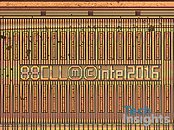
Source: Tech Insights
Add your own comment

28 Comments on Intel 10 nm Process Increases Transistor Density by 2.7x Over 14 nm: Report

#1
R0H1T
Not to forget it's still MIA. As an aside if there's 14nm+++ incoming, I wonder how bad 10nm (yields) could really be?
Posted on Reply
#2
prnsforum
STFU !! just release 9 series already
Posted on Reply
#3
RejZoR
I'm assuming Intel's 10nm is somewhat the same thing as GloFo (or TSMC?) 7nm given how things were in the past?
Posted on Reply
#4
las
Yes Intel 10nm = TSMC/GloFo 7nm

Intel 14nm is more advanced than GloFo 12nm (Ryzen refresh)

I expect Intel 10nm by late 18 or early 19. Intel might get in trouble if not ready for Zen 2 release. We have started seeing Intel small die 10nm chips, looks like progress
Posted on Reply
#5
ShurikN
RejZoRI'm assuming Intel's 10nm is somewhat the same thing as GloFo (or TSMC?) 7nm given how things were in the past?
From every piece of info I've seen, both GloFo and TSMC 7nm are slightly superior to Intel's 10nm.
But the thing is, when Intel releases mass produced 10nm products, it'll be on 10nm+ or some sort of evolution/optimization. So that one might be better than standard 7nm. Then again the competition will move to 7nm+ EUV or whatever it's gonna be. It's gonna go back and forth.
Posted on Reply
#6
bug
R0H1TNot to forget it's still MIA. As an aside if there's 14nm+++ incoming, I wonder how bad 10nm (yields) could really be?
It's not available in quantity, but you do realize this article is based on taking a 10nm die and putting it under the microscope.
Also, for all its troubles, if the end result is an almost 3x density, Intel will have quite the advantage over the competition once they fully flesh 10nm out. And I'm pretty sure at their next node, everybody else will need to figure out quad-patterning as well.
Posted on Reply
#7
iO
And yet this high density is what bit them in the 10nm arse so they went back to a scaling factor of 2.4x for 7nm.
Posted on Reply
#8
londiste
iOAnd yet this high density is what bit them in the 10nm arse so they went back to a scaling factor of 2.4x for 7nm.
Scaling factor of 2.4x is still very-very aggressive. That one is likely to bite them in the ass again when the time comes. Probably in the form of long delays. Again.
Posted on Reply
#9
kastriot
Now just cut down prices 2.7x and here we go..
Posted on Reply
#10
bug
kastriotNow just cut down prices 2.7x and here we go..
Unfortunately, after all these woes, price cuts are rather (highly?) unlikely. I wouldn't mind being proven wrong, though ;)
Posted on Reply
#11
R0H1T
bugIt's not available in quantity, but you do realize this article is based on taking a 10nm die and putting it under the microscope.
Also, for all its troubles, if the end result is an almost 3x density, Intel will have quite the advantage over the competition once they fully flesh 10nm out. And I'm pretty sure at their next node, everybody else will need to figure out quad-patterning as well.
Yes & according to Intel own estimates 14nm++ is still better than 10nm or 10nm+ (marginally with the latter) so in terms of process characteristics (performance) ICL is going to fall short wrt best of CFL.

In short density isn't everything, in fact when you're packing billions of transistors it's best to look elsewhere for other advantages wrt competition in GF & TSMC.
Posted on Reply
#12
bug
The first graph show transistor performance. If the transistor performance is only slightly lower, but you can have almost 3x as many transistors, I'd say the resulting chip has a good chance at being faster.

Fwiw, that graph also says14nm++ is leaps and bounds faster than plain 14nm. But we all know the resulting CPUs aren't.
Posted on Reply
#13
R0H1T
bugThe first graph show transistor performance. If the transistor performance is only slightly lower, but you can have almost 3x as many transistors, I'd say the resulting chip has a good chance at being faster.

Fwiw, that graph also says14nm++ is leaps and bounds faster than plain 14nm. But we all know the resulting CPUs aren't.
The problem with such high density is that in real world your chips will not be able to clock super high, like CFL, because even if 14nm++ is way better than 14nm or 14nm+ it wasn't designed to clock up to 5GHz (base clock) for 6 or more cores. So while ICL would improve over CFL, the upper limit as far as clock speed, including realistic overclocks, should be interesting to say the least.
Posted on Reply
#14
londiste
I wonder what the "Higher Performance" in these slides refers to. Slight increases in both density and clocks?
Intel's 14nm as a process probable maxes out at around 5 GHz for the frequency. At reasonable voltage/power consumption, that is. And this does not seem to depend on the size at all.

At the same time, both density and lower power are what drives everyone including Intel to smaller node.
Posted on Reply
#15
bug
R0H1TThe problem with such high density is that in real world your chips will not be able to clock super high, like CFL, because even if 14nm++ is way better than 14nm or 14nm+ it wasn't designed to clock up to 5GHz (base clock) for 6 or more cores. So while ICL would improve over CFL, the upper limit as far as clock speed, including realistic overclocks, should be interesting to say the least.
Which is why instead of trying to predict performance. I'm just waiting to see the chips. Probably won't upgrade anyway, so I'm super chill about it :D
Posted on Reply
#16
R0H1T
bugWhich is why instead of trying to predict performance. I'm just waiting to see the chips. Probably won't upgrade anyway, so I'm super chill about it :D
Hence my assumption that Intel's in a lot of trouble, I wonder if gamers will give up their 5~5.5GHz OC water cooled CFL for a 5~10% reduction in clock speeds at 10nm?
Anyway the point is 10nm is turning out to be a bigger can of worms than what Intel could've ever imagined, even in their worst nightmares.
Posted on Reply
#17
bug
R0H1THence my assumption that Intel's in a lot of trouble, I wonder if gamers will give up their 5~5.5GHz OC water cooled CFL for a 5~10% reduction in clock speeds at 10nm?
Ice Lake is supposed to be a new architecture, direct clocks comparison might not apply.
Posted on Reply
#18
ppn
How does this CPU prove the concept of 10nm with. 127 sq.mm and is only Dual_core. FFS Intel 6-Core is 149 sq.mm.

If anything I would expect 6-Core on 10nm to be shrinked to 50 sq.mm. not Dualcore to be 127.
Posted on Reply
#19
londiste
ppnHow does this CPU prove the concept of 10nm with. 127 sq.mm and is only Dual_core. FFS Intel 6-Core is 149 sq.mm.
If anything I would expect 6-Core on 10nm to be shrinked to 50 sq.mm. not Dualcore to be 127.
The small Cannon Lake we have seen should be ~70 mm² and that includes a 40 EU iGPU.
For comparison, the same 2 cores along with 24 EU iGPU in Kaby Lake are 127 mm² at 14 nm process.
Posted on Reply
#20
R0H1T
ppnHow does this CPU prove the concept of 10nm with. 127 sq.mm and is only Dual_core. FFS Intel 6-Core is 149 sq.mm.

If anything I would expect 6-Core on 10nm to be shrinked to 50 sq.mm. not Dualcore to be 127.
A lot of the stuff on a chip doesn't scale down like the actual cores with a node shrink, lots of uncore elements IIRC.
Posted on Reply
#21
Vya Domus
londisteScaling factor of 2.4x is still very-very aggressive.
Is it though ? Somehow Samsung , TSMC and GloFo all have managed to achieve higher density and significantly better yields than Intel as of now. It's not that the node shrink was too aggressive , they bit off more than what they could chew. You simply cannot beat companies that dedicate all their cash to R&D and new plants anymore.
Posted on Reply
#22
londiste
Vya DomusIs it though ? Somehow Samsung , TSMC and GloFo all have managed to achieve higher density and significantly better yields than Intel as of now. It's not that the node shrink was too aggressive , they bit off more than what they could chew. You simply cannot beat companies that dedicate all their cash to R&D and new plants anymore.
Samsung, TSMC and GloFo are all doing smaller steps. 14 > 12/10 > 7. Intel went 14 > 10.
Granted, GloFo seems to be planning to skip 7 nm and go straight to 5 nm but we will see how this goes.

At this point, TSMC and GloFo actually seem to be having slightly lower transistor density at respective 7 nm processes than Intel at 10 nm. Samsung has a bit better but their 7 nm is at about the same stage where Intel is with 10 nm. We don't know much about yields beyond the fact that TSMC is doing volume production which we can assume means OK yields.

Production process is the foundation of entire Intel business, not just CPUs. We can safely say Intel is putting everything it can into making their 10 nm process work to stay competitive.
Posted on Reply
#23
jabbadap
londisteSamsung, TSMC and GloFo are all doing smaller steps. 14 > 12/10 > 7. Intel went 14 > 10.
Granted, GloFo seems to be planning to skip 7 nm and go straight to 5 nm but we will see how this goes.

At this point, TSMC and GloFo actually seem to be having slightly lower transistor density at respective 7 nm processes than Intel at 10 nm. Samsung has a bit better but their 7 nm is at about the same stage where Intel is with 10 nm. We don't know much about yields beyond the fact that TSMC is doing volume production which we can assume means OK yields.

Production process is the foundation of entire Intel business, not just CPUs. We can safely say Intel is putting everything it can into making their 10 nm process work to stay competitive.
Well GloFo skipped "10nm" and went straight trough the "7nm". There is a rumor they might skip the "5nm" as well and go straight do the "3nm".
Posted on Reply
#24
piloponth
"100.8 million transistors per square millimeter"

jesus, can you imagine that. Some of the simpler chips (remember, Pentium III had 9.5 million transistors) can be manufactured in submilimeter sizes.
Posted on Reply
#25
voltage
prnsforumSTFU !! just release 9 series already
SPOT ON. thank you
Posted on Reply
Add your own comment
Apr 26th, 2024 11:50 EDT change timezone

New Forum Posts

Popular Reviews

Controversial News Posts