Wednesday, July 21st 2021

NVIDIA Multi-Chip-Module Hopper GPU Rumored To Tape Out Soon

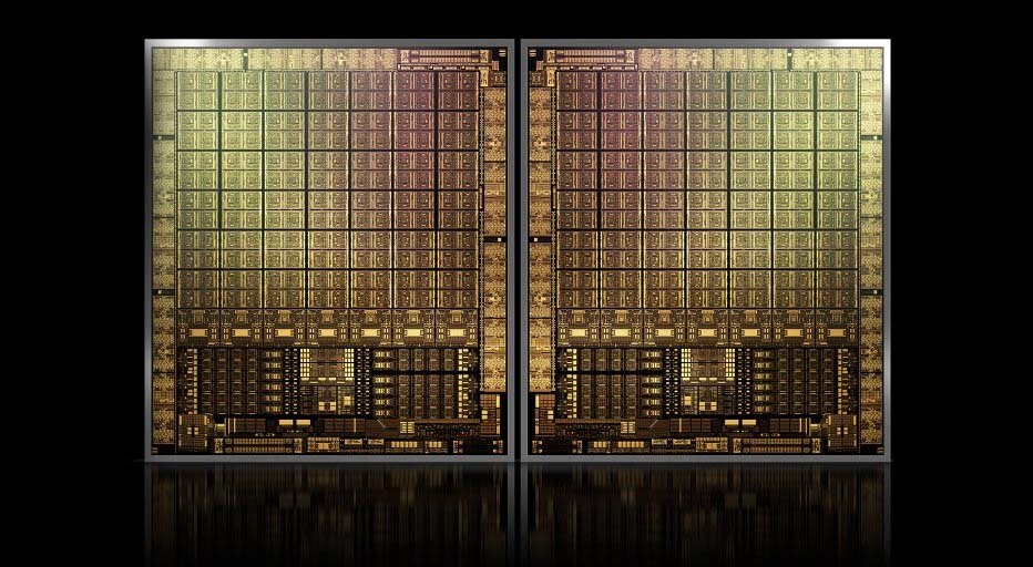
Hopper is an upcoming compute architecture from NVIDIA which will be the first from the company to feature a Multi-Chip-Module (MCM) design similar to Intel's Xe-HPC and AMD's upcoming CDNA2. The Hopper architecture has been teased for over 2 years but it would appear that it is nearing completion with a recent leak suggesting the product will tape out soon. This compute GPU will likely be manufactured on TSMC's 5 nm node and could feature two dies each with 288 Streaming Microprocessors which could theoretically provide a three-fold performance improvement over the Ampere-based NVIDIA A100. The first product to feature the GPU is expected to be the NVIDIA H100 data center accelerator which will serve as a successor to the A100 and could potentially launch in mid-2022.
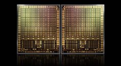
Sources: @3DCenter_org, VideoCardz
Add your own comment

35 Comments on NVIDIA Multi-Chip-Module Hopper GPU Rumored To Tape Out Soon

#26
InVasMani
AquinusThat's what people said about CPUs using MCM. Those are problems to be solved, not ones to be avoided. With that said, I don't see MCM being unrealistic for GPUs. It'll just take time to get right.
It can't possibly be any worse than Lucid Hydra or SLI/CF what do they have to loose!!? For starters the more recent PCI-E bus along with infinity cache, resizable bar, direct storage, ect not to mention modern insanely multi core CPU's makes it more flexible than those other examples done in the past on slower everything above.

Even if not perfect I'm sure MCM will be better than past paired GPU mixing solutions in history unless these companies are just plain incompetent and learned nothing of value from the past attempts.
Posted on Reply
#27
Aquinus
Resident Wat-man
InVasManiIt can't possibly be any worse than Lucid Hydra or SLI/CF what do they have to loose!!? For starters the more recent PCI-E bus along with infinity cache, resizable bar, direct storage, ect not to mention modern insanely multi core CPU's makes it more flexible than those other examples done in the past on slower everything above.

Even if not perfect I'm sure MCM will be better than past paired GPU mixing solutions in history unless these companies are just plain incompetent and learned nothing of value from the past attempts.
Exactly. GPU manufacturers have already demonstrated an ability to do this with GPUs with their own memory and a considerable distance between the two chips and their memory. Latency is a very real problem (micro-stutter anyone?) but those are also issues that can be mitigated, even in SLI/Crossfire setups. That's a very different animal when instead of having two GPUs with two pools of memory talking over a relatively long PCIe link, think about two GPU chiplets and an I/O die like AMD does with their CPUs now with common GPU memory between the two dies. Latency will be far better than talking over PCIe, shared memory means no copying to another pool of memory, and direct access to the I/O die means that that I/O die can be responsible for handling output to displays.

All in all, I think going this route is a no-brainer from a scalability standpoint. The real issue is cost because it's a more complicated process to do MCM if you're not already doing it at scale. AMD kind of has a leg up on this because they're already doing it and are far further along than just having multiple dies on a chip. The I/O chip with more simple chiplets was a game changer to be honest and I think we'll see that kind of design drive future high performance GPU designs.

All in all, I think nVidia is about where Intel is on the MCM path. They have multiple dies per chip, but they're still doing the direct communication thing which doesn't scale as well as AMD's solution does. It works okay for two dies, 4 dies is complicated and costly (forget the latency penalty talking to a die you don't have a direct connection to,) and any more is inefficient. However with the I/O die, we've seen how many chiplets AMD can cram on to a single chip. Smaller dies are easier to produce consistently with better yields as well.

This is a slight tangent, but what I would like to see is AMD produce a CPU where the chiplets are mixed between CPU and GPU chiplets. We could finally see some really interesting APUs out of AMD if they did.
Posted on Reply
#28
Lycanwolfen
Hmmmm I'm trying to remember who tried putting two GPU's on a single card. Something 20 years ago. Let me think. Oh wait Now I know the Voodoo 5 5500 AGP by 3dfx. Which Nvidia bought to have SLI. Then what did 3dfx do they said SLI was dead and tried to put everything on a single card. Why is history repeating itself.
Posted on Reply
#29
Aquinus
Resident Wat-man
LycanwolfenHmmmm I'm trying to remember who tried putting two GPU's on a single card. Something 20 years ago. Let me think. Oh wait Now I know the Voodoo 5 5500 AGP by 3dfx. Which Nvidia bought to have SLI. Then what did 3dfx do they said SLI was dead and tried to put everything on a single card. Why is history repeating itself.
It's happened a few times since. I think the most recent on the AMD side is the 295X2. The real kicker is having two pools of GPU memory. That's a solvable problem with an MCM design.
www.techpowerup.com/gpu-specs/radeon-r9-295x2.c2523
Posted on Reply
#30
InVasMani
AquinusExactly. GPU manufacturers have already demonstrated an ability to do this with GPUs with their own memory and a considerable distance between the two chips and their memory. Latency is a very real problem (micro-stutter anyone?) but those are also issues that can be mitigated, even in SLI/Crossfire setups. That's a very different animal when instead of having two GPUs with two pools of memory talking over a relatively long PCIe link, think about two GPU chiplets and an I/O die like AMD does with their CPUs now with common GPU memory between the two dies. Latency will be far better than talking over PCIe, shared memory means no copying to another pool of memory, and direct access to the I/O die means that that I/O die can be responsible for handling output to displays.

All in all, I think going this route is a no-brainer from a scalability standpoint. The real issue is cost because it's a more complicated process to do MCM if you're not already doing it at scale. AMD kind of has a leg up on this because they're already doing it and are far further along than just having multiple dies on a chip. The I/O chip with more simple chiplets was a game changer to be honest and I think we'll see that kind of design drive future high performance GPU designs.

All in all, I think nVidia is about where Intel is on the MCM path. They have multiple dies per chip, but they're still doing the direct communication thing which doesn't scale as well as AMD's solution does. It works okay for two dies, 4 dies is complicated and costly (forget the latency penalty talking to a die you don't have a direct connection to,) and any more is inefficient. However with the I/O die, we've seen how many chiplets AMD can cram on to a single chip. Smaller dies are easier to produce consistently with better yields as well.

This is a slight tangent, but what I would like to see is AMD produce a CPU where the chiplets are mixed between CPU and GPU chiplets. We could finally see some really interesting APUs out of AMD if they did.
AMD already has APU's what they could mix is two different APU chiplets though in a big.LITTLE type of scenario. Basically the base frequency and boost frequency of two chiplets could have overlap and convergence giving a spectrum mixture of performance and efficiency and a larger convergence at the middle.
Posted on Reply
#31
Aquinus
Resident Wat-man
InVasManiAMD already has APU's what they could mix is two different APU chiplets though in a big.LITTLE type of scenario. Basically the base frequency and boost frequency of two chiplets could have overlap and convergence giving a spectrum mixture of performance and efficiency and a larger convergence at the middle.
I'm not thinking of two APU chiplets, but rather one chiplet being the CPU cores and the other being the GPU cores, both sharing the same I/O die in the middle.
Posted on Reply
#32
InVasMani
That would work too I suppose, but you couldn't do as much with power savings in that scenario. A a example stuff like Nvidia's Optimus tech for laptops wouldn't be possible with that approach. You could go headless on the GPU I suppose, but that's more likely to happen in a server environment as opposed to consumer orientated devices. I'd rather be able to turn off the stronger or weaker chip entirely in some kind of deep sleep state to better conserve power.

I fail to see any performance to be gained from it if the underlying hardware adds up to the same amount as well. I suppose it might provide scenario's where you can do twice the work in single clock cycle off the CPU/GPU perhaps? If that's the angle you were going towards then maybe idk honestly. I still think the potential power savings of just two APU chiplets would make better sense overall. Just what that would bring for AMD in the mobile market alone is significant and hard to overlook.
AquinusIt's happened a few times since. I think the most recent on the AMD side is the 295X2. The real kicker is having two pools of GPU memory. That's a solvable problem with an MCM design.
www.techpowerup.com/gpu-specs/radeon-r9-295x2.c2523
I think that's one of the significant things DX12 brought about that was intended to help with mGPU was pooled memory. Just wait til pooled memory, direct storage, and infinity cache are combined with mGPU things will start to heat up.
Posted on Reply
#33
80251
AquinusIt's happened a few times since. I think the most recent on the AMD side is the 295X2. The real kicker is having two pools of GPU memory. That's a solvable problem with an MCM design.
www.techpowerup.com/gpu-specs/radeon-r9-295x2.c2523
The Radeon Pro Duo is the most recent gaming capable dual-GPU design from AMD, that was back in 2016 though.
Posted on Reply
#34
Aquinus
Resident Wat-man
InVasManiI think that's one of the significant things DX12 brought about that was intended to help with mGPU was pooled memory. Just wait til pooled memory, direct storage, and infinity cache are combined with mGPU things will start to heat up.
I think that's a solution to the SLI/Crossfire problem, for sure. If GPU memory is shared, that no longer is an issue and actually solves one of the biggest problems with multi-GPU setups. The biggest cost is communication between the two dies to keep memory in sync. There are bandwidth and latency limitations on that front. Think about it, if both GPUs share memory, they can render and apply their changes directly to the same framebuffer for output. Microstutter would become a thing of the past.
80251The Radeon Pro Duo is the most recent gaming capable dual-GPU design from AMD, that was back in 2016 though.
Ah yeah, I forgot about that one. Still, 5 years ago isn't that long.
Posted on Reply
#35
InVasMani
Place a single CPU core on each GPU chiplet designed around compression/decompression that has infinity cache and use direct storage and shared memory pool.
Posted on Reply
Add your own comment
Apr 25th, 2024 23:31 EDT change timezone

New Forum Posts

Popular Reviews

Controversial News Posts