Monday, October 12th 2026

GlobalFoundries Returns to Advanced-Node Race With 7 nm-Class FDX Fusion
Back in the now distant 2018, the semiconductor industry had three major players in contract leading-edge node manufacturing: TSMC, Samsung, and GlobalFoundries. At that time, Intel did not accept external clients. However, as node design became increasingly expensive—requiring multi-billion dollar investments—and more complex, with many players encountering yield and manufacturing difficulties, GlobalFoundries announced that it was stopping its 7 nm node development indefinitely. This left only two companies in the leading-edge race, but GlobalFoundries continued to develop unique semiconductor solutions that did not focus on smaller transistor sizes.
Today, the company is back at a similar stopping point but with a unique solution called FDX Fusion, based on fully-depleted silicon-on-insulator (FD-SOI) technology. Unlike traditional CMOS, GlobalFoundries takes substrate isolation a step further by creating a fully insulating layer beneath the channel. This enables highly specialized capabilities, such as ultra-low-power in-memory computing, seamless integration of embedded non-volatile memory (like eMRAM), and highly efficient dense logic designs. With FDX Fusion, GlobalFoundries claims 7 nm-class node characteristics in terms of size and twice the transistor density of the first-generation 22FDX node, which was designated as a 22 nm-class design.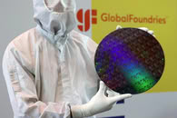 For manufacturing, GlobalFoundries plans to start FDX Fusion mass production in 2028 at its advanced facility in Dresden, Germany. This facility will be one of the strongest manufacturing regions in Europe, making chip sovereignty another important factor with the start of mass production. Customers can expect to receive initial technology demos next year, with PDK shipping in mid-2027. GlobalFoundries sees this node as a highly specialized solution for physical AI layers, applicable in areas from automotive and ASIC to the physical world, with sensing, heavy computations, and new requirements.
Source:
GlobalFoundries
Today, the company is back at a similar stopping point but with a unique solution called FDX Fusion, based on fully-depleted silicon-on-insulator (FD-SOI) technology. Unlike traditional CMOS, GlobalFoundries takes substrate isolation a step further by creating a fully insulating layer beneath the channel. This enables highly specialized capabilities, such as ultra-low-power in-memory computing, seamless integration of embedded non-volatile memory (like eMRAM), and highly efficient dense logic designs. With FDX Fusion, GlobalFoundries claims 7 nm-class node characteristics in terms of size and twice the transistor density of the first-generation 22FDX node, which was designated as a 22 nm-class design.

8 Comments on GlobalFoundries Returns to Advanced-Node Race With 7 nm-Class FDX Fusion
A 3090 on this node would be interesting.**
**no, it wouldn't performance is just 7nm like, it's nothing like 7nm I should have read more carefully
Let's hope the $1.5B was worth it
I am reading they tried going to 12nm FDX, but canceled it. Now they are trying to go one step further.
Someone shoot this sick dog.