News Posts matching #22 nm

Return to Keyword Browsing

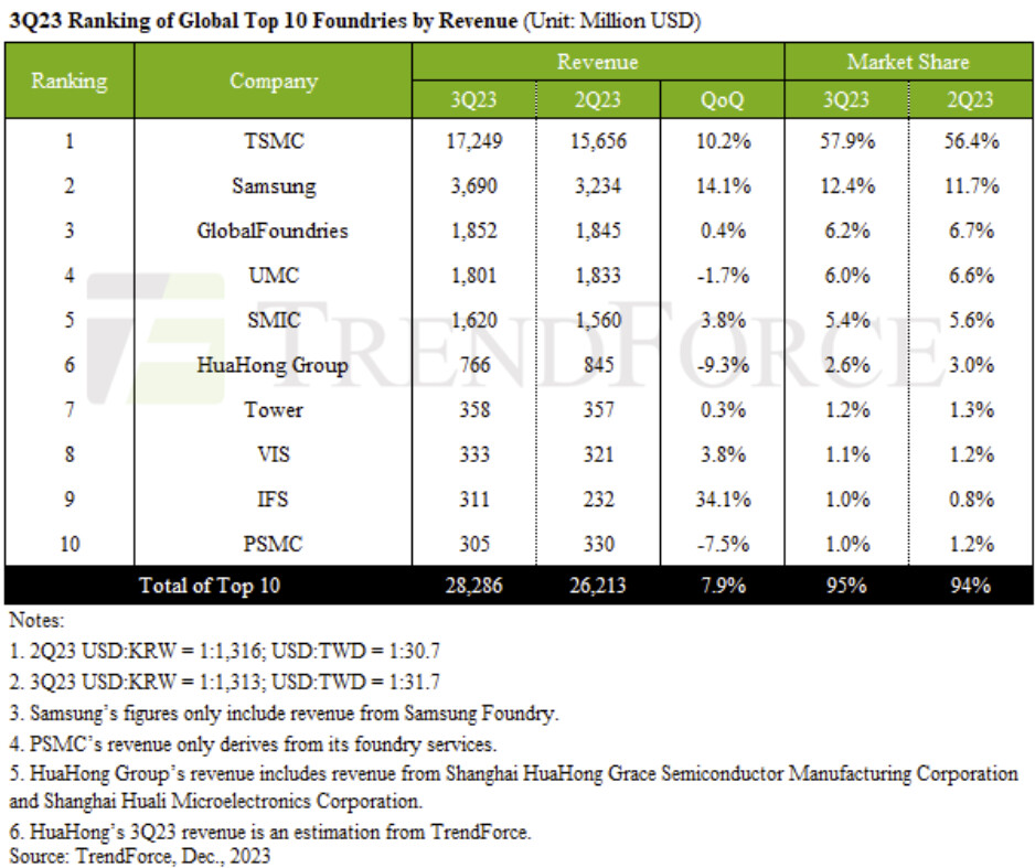
Phison Launches Full Range of UFS Storage Solutions for Unparalleled Mobile Storage Performance

Phison Electronics, a leading provider of NAND controllers and NAND storage solutions, today announced it has introduced a full range of UFS (Universal Flash Storage) controllers (PS8325, PS8327, PS8329, PS8361). Phison's new UFS solutions support entry-level, middle, premium and flagship smartphone devices to achieve maximum performance in mobile storage and enhance user experiences.

As smartphone devices require higher performance, the storage devices of many entry-level 5G models have transitioned from eMMC to UFS 2.2 storage, and even flagship models of 4G phones have begun adopting the UFS 2.2 specification. Compared to the half-duplex mode of eMMC, the full-duplex mode of UFS 2.2 significantly increases read speeds by three times, not only handling smartphone functions that require processing large amounts of data (such as high-resolution recording and video playback), but also consuming lower power under the same performance speed as eMMC. This helps improve the battery life of smartphones and tablets, meeting the high-performance and low-power consumption needs of mobile devices.

Chinese Researchers Want to Make Wafer-Scale RISC-V Processors with up to 1,600 Cores

According to the report from a journal called Fundamental Research, researchers from the Institute of Computing Technology at the Chinese Academy of Sciences have developed a 256-core multi-chiplet processor called Zhejiang Big Chip, with plans to scale up to 1,600 cores by utilizing an entire wafer. As transistor density gains slow, alternatives like multi-chiplet architectures become crucial for continued performance growth. The Zhejiang chip combines 16 chiplets, each holding 16 RISC-V cores, interconnected via network-on-chip. This design can theoretically expand to 100 chiplets and 1,600 cores on an advanced 2.5D packaging interposer. While multi-chiplet is common today, using the whole wafer for one system would match Cerebras' breakthrough approach. Built on 22 nm process technology, the researchers cite exascale supercomputing as an ideal application for massively parallel multi-chiplet architectures.

Careful software optimization is required to balance workloads across the system hierarchy. Integrating near-memory processing and 3D stacking could further optimize efficiency. The paper explores lithography and packaging limits, proposing hierarchical chiplet systems as a flexible path to future computing scale. While yield and cooling challenges need further work, the 256-core foundation demonstrates the potential of modular designs as an alternative to monolithic integration. China's focus mirrors multiple initiatives from American giants like AMD and Intel for data center CPUs. But national semiconductor ambitions add urgency to prove domestically designed solutions can rival foreign innovation. Although performance details are unclear, the rapid progress shows promise in mastering modular chip integration. Combined with improving domestic nodes like the 7 nm one from SMIC, China could easily create a viable Exascale system in-house.

Top 10 Foundries Experience 7.9% QoQ Growth in 3Q23, with a Continued Upward Trend Predicted for Q4

TrendForce's research indicates a dynamic third quarter for the global foundry industry, marked by an uptick in urgent orders for smartphone and notebook components. This surge was fueled by healthy inventory levels and the release of new iPhone and Android devices in 2H23. Despite persisting inflation risks and market uncertainties, these orders were predominantly executed as rush orders. Additionally, TSMC and Samsung's high-cost 3 nm manufacturing process had a positive impact on revenues, driving the 3Q23 value of the top ten global foundries to approximately US$28.29 billion—a 7.9% QoQ increase.

Looking ahead to 4Q23, the anticipation of year-end festive demand is expected to sustain the inflow of urgent orders for smartphones and laptops, particularly for smartphone components. Although the end-user market is yet to fully recover, pre-sales season stockpiling for Chinese Android smartphones appears to be slightly better than expected, with demand for mid-to-low range 5G and 4G phone APs and continued interest in new iPhone models. This scenario suggests a continued upward trend for the top ten global foundries in Q4, potentially exceeding the growth rate seen in Q3.

Winbond Introduces Innovative CUBE Architecture for Powerful Edge AI Devices

Winbond Electronics Corporation, a leading global supplier of semiconductor memory solutions, has unveiled a powerful enabling technology for affordable Edge AI computing in mainstream use cases. The Company's new customized ultra-bandwidth elements (CUBE) enable memory technology to be optimized for seamless performance running generative AI on hybrid edge/cloud applications.

CUBE enhances the performance of front-end 3D structures such as chip on wafer (CoW) and wafer on wafer (WoW), as well as back-end 2.5D/3D chip on Si-interposer on substrate and fan-out solutions. Designed to meet the growing demands of edge AI computing devices, it is compatible with memory density from 256 Mb to 8 Gb with a single die, and it can also be 3D stacked to enhance bandwidth while reducing data transfer power consumption.

Top 10 Foundries Report Nearly 20% QoQ Revenue Decline in 1Q23, Continued Slide Expected in Q2

TrendForce reports that the global top 10 foundries witnessed a significant 18.6% QoQ decline in revenue during the first quarter of 2023. This decline—amounting to approximately US$27.3 billion—can be attributed to sustained weak end-market demand and the compounded effects of the off-peak season. The rankings also underwent notable changes, with GlobalFoundries surpassing UMC to secure the third position, and Tower Semiconductor surpassing PSMC and VIS to claim the seventh spot.

Declining capacity utilization rate and shipment volume contribute to widened revenue decline
The revenue decline in Q1 was primarily influenced by declining capacity utilization rates and shipment volume across the top 10 foundries. For instance, TSMC generated US$16.74 billion in revenue—marking a 16.2% QoQ drop in revenue. Weakened demand for mainstream applications such as laptops and smartphones led to a significant decline in the utilization rates and revenue of the 7/6 nm and 5/4 nm processes, falling over 20% and 17%, respectively. While the second quarter may see temporary relief coming from rush orders, the persistently low capacity utilization rate indicates that revenue is likely to continue declining, albeit at a slower pace compared to Q1.

Strict Restrictions Imposed by US CHIPS Act Will Lower Willingness of Multinational Suppliers to Invest

TrendForce reports that the US Department of Commerce recently released details regarding its CHIPS and Science Act, which stipulates that beneficiaries of the act will be restricted in their investment activities—for more advanced and mature processes—in China, North Korea, Iran, and Russia for the next ten years. The scope of restrictions in this updated legislation will be far more extensive than the previous export ban, further reducing the willingness of multinational semiconductor companies to invest in China for the next decade.

CHIPS Act will mainly impact TSMC; and as the decoupling of the supply chain continues, VIS and PSMC capture orders rerouted from Chinese foundries
In recent years, the US has banned semiconductor exports and passed the CHIPS Act, all to ensure supply chains decoupling from China. Initially, bans on exports were primarily focused on non-planar transistor architecture (16/14 nm and more advanced processes). However, Japan and the Netherlands have also announced that they intend to join the sanctions, which means key DUV immersion systems, used for producing both sub-16 nm and 40/28 nm mature processes, are likely to be included within the scope of the ban as well. These developments, in conjunction with the CHIPS Act, mean that the expansion of both Chinese foundries and multinational foundries in China will be suppressed to varying degrees—regardless of whether they are advanced or mature processes.

UMC Reports Fourth Quarter 2022 Results

United Microelectronics Corporation ("UMC" or "The Company"), a leading global semiconductor foundry, today announced its consolidated operating results for the fourth quarter of 2022. Fourth quarter consolidated revenue was NT$67.84 billion, decreasing 10.0% QoQ from NT$75.39 billion in 3Q22. Compared to a year ago, 4Q22 revenue grew 14.8% YoY from NT$59.10 billion in 4Q21. Consolidated gross margin for 4Q22 was 42.9%. Net income attributable to the shareholders of the parent was NT$19.1 billion, with earnings per ordinary share of NT$1.54.

Jason Wang, co-president of UMC, said, "In the fourth quarter, due to a significant slowdown across most of our end markets and inventory correction in the semiconductor industry, our wafer shipments fell 14.8% QoQ while overall fab utilization rate dropped to 90%. Average selling price increased slightly during the quarter as a result of our ongoing product mix optimization efforts, moderating the decline in revenue."

TSMC (Not Intel) Makes the Vast Majority of Logic Tiles on Intel "Meteor Lake" MCM

Intel's next-generation "Meteor Lake" processor is the first mass-production client processor to embody the company's IDM 2.0 manufacturing strategy—one of building processors with multiple logic tiles interconnected with Foveros and a base-tile (essentially an interposer). Each tile is built on a silicon fabrication process most suitable to it, so that the most advanced node could be reserved for the component that benefits from it the most. For example, while you need the SIMD components of the iGPU to be built on an advanced low-power node, you don't need its display controller and media engine to, and these could be relegated to a tile built on a less advanced node. This way Intel is able to maximize its use of wafers for the most advanced nodes in a graded fashion.

Japanese tech publication PC Watch has annotated the "Meteor Lake" SoC, and points out that the vast majority of the chip's tiles and logic die-area is manufactured on TSMC nodes. The MCM consists of four logic tiles—the CPU tile, the Graphics tile, the SoC tile, and the I/O tile. The four sit on a base tile that facilitates extreme-density microscopic wiring interconnecting the logic tiles. The base tile is built on the 22 nm HKMG silicon fabrication node. This tile lacks any logic, and only serves to interconnect the tiles. Intel has an active 22 nm node, and decided it has the right density for the job.

More Details Emerge on Mediatek's Intel Foundry Plans

Last week's news about Mediatek signing an agreement to use Intel's Foundry Services (IFS) led to some speculation as to what Mediatek would be manufacturing at IFS. Details have now emerged in the Taiwan press about Mediatek's plans and the first products will be using the Intel 16 process, what was previously known as its 22 nm node. As such, we're not talking about anything cutting edge or even remotely close, but that's hardly a problem for Mediatek, as the company makes a vast range of products suitable for the node.

MediaTek CEO Rick Tsai mentioned that IFS will be used for producing semiconductors for digital TVs and wireless access networks at an investor conference in Taiwan. This suggests that most of the components might not even be for Mediatek itself, but rather its subsidiaries, such as MStar or Airoha. MStar is a company that produces a wide range of lower-end smart TV chips, whereas Airoha has ended up taking over Mediatek's networking and Bluetooth business units. Admittedly, Mediatek still has some of these types of products under its own brand, but these tend to be higher-end products that would require a more advanced node than 22 nm in most cases. Mediatek's move to IFS has raised concerns in Taiwan that the smaller foundries might be losing business from Mediatek over time, which means that UMC and PSMC are going to be on the losing end of this deal.

Qualcomm Launches Snapdragon W5+ and W5 Platforms for Next Generation Wearables

Qualcomm Technologies, Inc. today unveiled the latest additions to the company's suite of premium wearable platforms, Snapdragon W5+ Gen 1 and Snapdragon W5 Gen 1. These platforms are designed to advance ultra-low power and breakthrough performance for next generation connected wearables with a focus on extended battery life, premium user experiences, and sleek, innovative designs. By using these platforms, manufacturers can scale, differentiate, and develop products faster in the continuously growing and segmenting wearables industry.

New enhancements to the flagship Snapdragon W5+ platform offer 50% lower power, 2X higher performance, 2X richer features, and 30% smaller size, compared to our previous generation, enabling wearable manufacturers to deliver the differentiated experiences consumers demand. Based on the hybrid architecture, the purpose-built platform is comprised of a 4 nm-based system-on-chip and 22 nm-based highly integrated always-on co-processor. It incorporates a series of platform innovations including new ultra-low power Bluetooth 5.3 architecture, low power islands for Wi-Fi, GNSS, and Audio, and low power states such as Deep Sleep and Hibernate.

Intel and QuTech Demonstrate Advances in Solving Quantum Interconnect Bottlenecks

Today, Intel and QuTech—a collaboration between Delft University of Technology and the Netherlands Organisation for Applied Scientific Research - published key findings in quantum research to address the "interconnect bottleneck" that exists between quantum chips that sit in cryogenic dilution refrigerators and the complex room-temperature electronics that control the qubits. The innovations were covered in Nature, the industry-leading science journal of peer-reviewed research, and mark an important milestone in addressing one of the biggest challenges to quantum scalability with Intel's cryogenic controller chip Horse Ridge.

"Our research results, driven in partnership with QuTech, quantitatively prove that our cryogenic controller, Horse Ridge, can achieve the same high-fidelity results as room-temperature electronics while controlling multiple silicon qubits. We also successfully demonstrated frequency multiplexing on two qubits using a single cable, which clears the way for simplifying the "wiring challenge" in quantum computing. Together, these innovations pave the way for fully integrating quantum control chips with the quantum processor in the future, lifting a major roadblock in quantum scaling," said Stefano Pellerano, principal engineer at Intel Labs.

Intel B460 and H410 Incompatibility with "Rocket Lake" Explained

Earlier this week, Intel shook the DIY PC market, particularly the vast mainstream segment, by revealing that its mid-tier B460 and entry-level H410 desktop motherboard chipsets will not be compatible with 11th Gen Core "Rocket Lake-S" processors, and that only its top-tier Z490 and H470, will. We have an explanation into what's going on, after consulting with people in the know, thanks to our friends at Hardware Zone Israel, who spoke with sources within Intel. It turns out, that some batches of B460 and H410 PCH dies are re-badged from older generations of PCH, and built on the 22 nm silicon fabrication process; whereas the Z490 and H470 are based on a newer generation that's built on 14 nm. This is similar to Intel's move to carve out the B365 chipset from the older H170.

In addition to being limited to an older version of Intel ME (Management Engine), the H460 and H410 PCH lack the ability to communicate with "Rocket Lake-S" processors over side-band, using PMSYNC/PMDN signals, a design change Intel introduced with the "Tiger Lake" and "Rocket Lake" microarchitectures. The chipsets faced no such limitation with "Comet Lake-S." Intel's decision to re-badge older 22 nm-class PCH silicon as B460 and H410 may have been dictated by the company's 14 nm node volume constraints. HotHardware reports that some motherboard vendors, such as GIGABYTE, found a clever (albeit expensive) way around this limitation, by creating "V2" revisions of their existing B460 and H410 motherboards, which actually use the 14 nm H470 chipset.

GLOBALFOUNDRIES Announces New 22FDX+ Platform, Extending FDX Leadership with Specialty Solutions for IoT and 5G Mobility

GLOBALFOUNDRIES (GF ), the world's leading specialty foundry, announced today at its Global Technology Conference the next generation of its FDXTM platform, 22FDX+, to meet the ever-growing need for higher performance and ultra-low power requirements of connected devices. GF's industry-leading 22FDX (22 nm FD-SOI) platform has realized $4.5 billion in design wins, with more than 350 million chips shipped to customers around the world.

GF's new 22FDX+ builds on the company's 22FDX platform, offering a broader set of features that provide high performance, ultra-low power, and specialty features and capabilities for the newest generation of designs. The differentiated offering will further empower customers to create chips that are specifically optimized for Internet of Things (IoT), 5G, automotive, and satellite communications applications.

Intel Core i5-L15G7 Lakefield Processor Spotted

Intel has been experimenting with a concept of mixing various types of cores in a single package with a design called Lakefield. With this processor, you would get a package of relatively small dimensions that are 12-by-12-by-1 millimeters withing very low TDP. Thanks to the Twitter user InstLatX64 (@InstLatX64) we have some GeekBench 5 results of the new Lakefield chip. The CPU in question is the Core i5-L15G7, a 5 core CPU without HyperThreading. The 5C/5T would be a weird configuration if only Lakefield wasn't meant for such configs. There are one "big" Sunny Cove core and four "small" Tremont cores built on the 10 nm manufacturing process. This is the so-called compute die, where only the CPU cores are present. The base dies containing other stuff like I/O controllers and PHYs, memory etc. is made on a low-cost node like 22 nm, where performance isn't the primary target. The whole chip is targeting the 5-7 W TDP range.

In the GeekBench 5 result we got, the Core i5-L15G7 is a processor that has a base frequency of 1.4 GHz, while in the test it reached as high as 2.95 GHz speeds. This is presumably for the big Sunny Cove cores, as Tremont cores are supposed to be slower. The cache configuration reportedly puts 1.5 MB of L2$ and 4 MB of L3$ for the CPUs. If we take a look at performance numbers, the chip scores 725 points in single-core tests, while the multi-core result is 1566 points. We don't know what is the targeted market and what it competes with, however, if compared to some offerings from Snapdragon, like the Snapdragon 835, it offers double the single-threaded performance with a similar multi-core score. If this is meant to compete with the more powerful Snapdragon offerings like the 8cx model, comparing the two results in Intel's fail. While the two have similar single-core performance, the Snapdragon 8cx leads by as much as 76.9% in a multi-core scenario, giving this chip a heavy blow.
Intel Core i5-L15G7 Intel Lakefield

Everspin Technologies and GLOBALFOUNDRIES Extend MRAM Joint Development Agreement to 12nm

Everspin Technologies, Inc., the world's leading developer and manufacturer of Magnetoresistive RAM (MRAM), today announced an amendment of its Spin-transfer Torque (STT-MRAM) joint development agreement (JDA) with GLOBALFOUNDRIES (GF ), the world's leading specialty foundry. Everspin and GF have been partners on 40 nm, 28 nm, and 22 nm STT-MRAM development and manufacturing processes and have now updated their agreement to set the terms for a future project on an advanced 12 nm FinFET MRAM solution. Everspin is in production of discrete STT-MRAM solutions on 40 and 28 nm, including its award winning 1 Gb DDR4 device. GF recently announced it has achieved initial production of embedded MRAM (eMRAM) on its 22FDX platform.

Intel and QuTech Detail "Horse Ridge," First Cryogenic Quantum Computing Control Chip

Intel Labs, in collaboration with QuTech ‑ a partnership between TU Delft and TNO (Netherlands Organization for Applied Scientific Research) ‑ outlines key technical features of its new cryogenic quantum control chip "Horse Ridge" in a research paper released at the 2020 International Solid-State Circuits Conference (ISSCC) in San Francisco. The paper unveils key technical capabilities of Horse Ridge that address fundamental challenges in building a quantum system powerful enough to demonstrate quantum practicality: scalability, flexibility and fidelity.

"Today, quantum researchers work with just a small number of qubits, using smaller, custom-designed systems surrounded by complex control and interconnect mechanisms. Intel's Horse Ridge greatly minimizes this complexity. By systematically working to scale to thousands of qubits required for quantum practicality, we're continuing to make steady progress toward making commercially viable quantum computing a reality in our future," said Jim Clarke, director of quantum hardware, Intel Labs.

Intel Core i5-L16G7 is the first "Lakefield" SKU Appearance, Possible Prelude to New Nomenclature?

Intel Core i5-L16G7 is the first commercial SKU that implements Intel's "Lakefield" heterogenous x86 processor architecture. This 5-core chip features one high-performance "Sunny Cove" CPU core, and four smaller "Tremont" low-power cores, with an intelligent scheduler balancing workloads between the two core types. This is essentially similar to ARM big.LITTLE. The idea being that the device idles most of the time, when lower-powered CPU cores can hold the fort; performance cores kick in only when really needed, until which time they remain power-gated. Thai PC enthusiast TUM_APISAK discovered the first public appearance of the i5-L16G7 in an unreleased Samsung device that has the Userbenchmark device ID string "SAMSUNG_NP_767XCL."

Clock speeds of the processor are listed as "1.40 GHz base, with 1.75 GHz turbo," but it's possible that the two core types have different clock-speed bands, just like the cores on big.LITTLE SoCs. Other key components of "Lakefield" include an iGPU based on the Gen11 graphics architecture, and an LPDDR4X memory controller. "Lakefield" implements Foveros packaging, in which high-density component dies based on newer silicon fabrication nodes are integrated with silicon interposers based on older fabrication processes, which facilitate microscopic high-density wiring between the dies. In case of "Lakefield," the Foveros package features a 10 nm "compute field" die sitting atop a 22 nm "base field" interposer.

Intel Rumored to be Courting GlobalFoundries for Some CPU Manufacturing

With its own silicon fabrication facilities pushed to their capacity limits, Intel is looking for third-party semiconductor foundries to share some of its supply load, and according to a WCCFTech report, its latest partner could be GlobalFoundries, which has a 14 nm-class fab in Upstate New York. If it goes through, the possible Intel-GloFo deal could see contract manufacturing commence within 2020.

GloFo's fab offers 14 nm FinFET and 12LPP, a refinement that's marketed as 12 nm. According to the report, Intel could use GloFo for manufacturing CPU dies, specifically its entry-level chips such as Core i3, Pentium, and Celeron. Intel is also known to shed its own manufacturing workload by contracting foundries for 14 nm core-logic (chipsets). In a bid to maximize 14 nm fab allocation for its CPUs, Intel also started making some of its 300-series chipsets on the older 22 nm process, which goes to show the company's appetite for 14 nm.

Continuing 14 nm Supply Shortages Lead Intel to Reintroduce Haswell-based, 22 nm Pentium G3420

"Nothing Really Ends" is the title of a song from dEUS, a Belgian "art-rock" band. And it would seem this applies all too well to the world of technology too. Intel has issued a Product Change Notification (PCN) which has changed the previously dead and buried, Haswell-era, 22 nm Pentium G3420 from its "Discontinued" status back to a worded "canceling this Product Discontinuance completely per new roadmap decision and enabling the product long term once again." Which means the Pentium G3420 will have a new lease of life, and will be available to customers until May 2020, with final shipments on December of the same year.

This is clearly an attempt from Intel to increase part availability for OEMs and system manufacturers, who have already been quoted as considering AMD due to both increases in performance and efficiency in their processors, as well as constrained supply from Intel, with giant Dell already having pointed the finger at Intel as a cause for their lower than expected revenue.

Intel's FinFET-Based Embedded MRAM is Ready for Production

A report via EETimes slates Intel's own working MRAM (Magnetoresistive Random-Access Memory) is ready for production in high-volume manufacturing. MRAM is a nonvolatile memory technology, meaning that it retains information even if there is a change in powerstate (ie, power loss), meaning that it's more akin to a storage device than to, say, RAM.

But why does MRAM matter, really? Well, MRAM is being developed as a long-term candidate to a universal memory solution, replacing both DRAM (a volatile memory technology) and NAND flash (a nonvolatile one), since node scaling with these technologies is becoming increasingly harder. MRAM promises better-scaling (at the foundry level) processes, with much higher yield rates. The fact that MRAM has been demonstrated to be able to achieve 1 ns settling times, better than the currently accepted theoretical limits for DRAM, and much higher write speeds (as much as thousands of times faster) compared to NAND flash.

Intel Launches B365 Express Chipset on 22nm Process, Possibly a Re-branded Z170

Intel today introduced the B365 Express desktop motherboard chipset as an in-between to its B360 Express and H370 Express chipsets. This model is part of Intel's optical enlargement of its motherboard chipsets to the 22 nm HKMG+ silicon fabrication node, to free up 14 nm++ for processors. Despite this, the TDP of the chipset remains unchanged at 6 Watts. The B365 has a couple of feature additions and subtractions over B360. To begin with it has a wider PCI-Express downstream root-complex, with 20 gen 3.0 lanes, on par with H370 Express. The B360, if you'll recall, only has 12 downstream PCIe lanes. This means B365 motherboards will have additional M.2 and U.2 connectivity.

According to the ARK specifications page for the B365 Express, this chip completely lacks integrated 10 Gbps USB 3.1 gen 2 connectivity. Perhaps the expanded downstream PCIe is really meant for motherboard vendors to use third-party USB 3.1 gen 2 controller chips. You still get eight 5 Gbps USB 3.0 ports (notice we didn't say USB 3.1 gen 1, because don't expect fast-charging features). The chipset also loses the latest generation Wireless AC integrated MAC. All of these point to the possibility of the B365 Express being a re-branded Z170 with locked CPU overclocking. Adding credence to this theory is the fact that while the B360 uses ME version 12, the B365 uses the older ME version 11. Much like the H310C, the B365 could include platform support for Windows 7.

Intel to Move Select Chipset Fabrication Back to 22nm in Wake of 14 nm Silicon Constraints

Things seem to be taking turns to the worse at Intel in accordance to Murphy's law. Not only was the company hit with a multitude of security flaws embedded in their CPUs, which puts their michroarchitecture design chops in jeopardy, but now they also have to contend with silicon fabrication snags. That Intel's 14 nm fabs are being hit with overwhelming demand for their output capacity is already a known quantity, with rising prices of Intel mainstream CPUs and reports of the company outsourcing 14 nm chip production to TSMC in a bid to increase availability - a first since the company became vertically integrated with both design and manufacturing of their own chips.

TSMC to Build Intel 14nm Processors and Chipsets

Try to wrap your head around Intel contracting TSMC to build some of its processors! With its own 14 nanometer silicon fabrication nodes under stress from manufacturing several generations of Core and Xeon processors simultaneously, leading to market shortages, Intel is looking to contract TSMC to manufacture some of its 14 nm products. Among these are certain models of its desktop processors, and several 300-series chipsets, including the H310, which are currently fabbed on Intel's last 22 nm node, that's probably being converted to 14 nm.

The TSMC contract appears to be moving faster than expected, with the Taiwanese fab eager to demonstrate its competence to Intel and secure future orders as the company is closer than ever in going fully or partly fabless. According to industry observers, Intel is staring at a 1:2 supply-demand ratio, for the countless chip it's building on 14 nm; which may have forced it to contract some of these chip designs to TSMC. Motherboard vendors expect Intel to sort out its supply issues by the end of 2018, with big help from TSMC.

Intel Shelves Z390 Express As We Knew It, Could Re-brand Z370 as Z390

Intel is rumored to have shelved the iteration of its upcoming Z390 Express chipset as earlier publicized, the one which had certain new hardware features. It could now re-brand the existing Z370 Express as Z390 Express and probably bolster its reference design with heftier CPU VRM specifications, to cope better with its upcoming 8-core LGA1151 processors. The Z370 Express is similar in feature-set to the brink of being identical to its predecessor, the Z270 Express. This move could impact certain new hardware features that were on the anvil, such as significantly more USB 3.1 gen 2/gen1 ports directly from the PCH, integrated WiFi MAC, and Intel SmartSound technology, which borrowed certain concepts from edge-computing to implement native speech-to-text conversion directly on the chipset, for improved voice control latency and reduced CPU overhead.

The reasons behind this move could be a combination of last-minute cost-benefit analyses by Intel's bean-counters, and having to mass-produce Z390 Express on the busier-than-expected 14 nm silicon fabrication node, as opposed to current 300-series chipsets being built on the 22 nm node that's nearing the end of its life-cycle. Intel probably needed the switch to 14 nm for the significant increases in transistor-counts arising from the additional USB controllers, the WiFi MAC, and the SmartSound logic. Intel probably doesn't have the vacant 14 nm node capacity needed to mass-produce the Z390 yet, as its transition to future processes such as 10 nm and 7 nm are still saddled with setbacks and delays; and redesigning the Z390 (as we knew it) on 22 nm may have emerged unfeasible (i.e. the chip may have ended up too big and/or too hot). The Z390 Express chipset block-diagram, which we published in our older article has been quietly removed from Intel's website. It's also rumored that this move could force AMD to rethink its plans to launch its Z490 socket AM4 chipset.

A Push for the Higher Margin: Intel Reportedly Discontinues Production of Its H310 Chipset

A report straight out of DigiTimes, citing industry sources, says that Intel has discontinued production of its H310 chipset. The decision has apparently stemmed from lower than expected production capacity for chipsets on the 14 nm process. When that happens, production focus must shift to a specific part: in this case, Intel obviously went with the option with the lower opportunity cost, and increased production of the Z370 chipset: the one with the increased feature-set, and, most likely than not, higher margins.

After a single month of tight supply for the H310 chipset, motherboard makers are now forced to use Intel's B360 chipset in their more cost-conscious options as well - a part which carries higher cost, and thus precludes manufacturers from hitting all the price points they usually would with a fully vertical Intel chipset lineup. Speculation has emerged claiming Intel suspended the supply of H310 because they have chosen to conduct a manufacturing process change from the tight-supply 14 nm (used across almost all of Intel's production stack, both consumer and enterprise) to a 22 nm fabrication technology. Further speculation places this constrained 14 nm supply as existent because of the delay in advancing to 10 nm, a process that Intel expected to be producing in volume by now (and since a while back, to be fair).
Return to Keyword Browsing
Apr 29th, 2024 22:41 EDT change timezone

New Forum Posts

Popular Reviews

Controversial News Posts