Saturday, October 20th 2007

ATI Radeon HD 3800 Series Specs, Photos and Logos

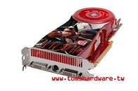
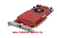
The title says it all. ATI Radeon HD 3870, the one on the second picture will feature 825MHz core and 2400MHz memory clocks, DirectX 10.1 support, and PCI-e 2.0 technology. ATI Radeon HD 2850 on the third picture will be clocked at 700MHz/1800MHz core/memory with DirectX 10.1 support and PCI-e 2.0. Both cards will feature 55nm manufactured graphics processing unit (GPU).
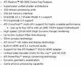
Sources: Tom's Hardware, VR-forums
Add your own comment

80 Comments on ATI Radeon HD 3800 Series Specs, Photos and Logos

#51
ChaoticBlankness
Urbklr911I think this is GAY.....what is wrong with AMD....why would they move to a new series....when they pretty much just gained some steam on the HD 2k series...
AMD is hoping to beat the GF 8000 series with these higher clocked cards, that's all. Is it right? No. Are they doing it anyways? Yes.

The trouble is we can all be mad out how misleading it is, but at the end of the day will that stop us from buying if the price/performance good? No.
Posted on Reply
#52
Tatty_Two
Gone Fishing
There are going to be an aweful lot of mid/mid high cards on the market in a couple of months to chose from, it will be interesting how they all fit into a pricing strategy:

8800GTS 320 G80
8800GTS 640 G80
8800GT G92 256
8800GT G92 512
8800GTS 640 with extra pipes (112) G80

etc etc

2900pro
2950pro
2900xt
2950xt???
2952.5 proX :D

I am lost already :cry:
Posted on Reply
#53
JC316
Knows what makes you tick
AphexDreamerHmmm, should I be mad that I just recently bought a HD2900Pro?
I'm not. The 2900 pro is awesome. The 2850 does look nice though, but I will still stick with my 2900.
Posted on Reply
#54
Urbklr
JC316I'm not. The 2900 pro is awesome. The 2850 does look nice though, but I will still stick with my 2900.
Correction......3850
This numbering is STILL GAY
Posted on Reply
#56
GrapeApe
15th WarlockAMD has finally lost it, using a higher number for a brand new next gen flagship video card has been a practice in the video card business since ever, for example Radeon 7200-8500-9700-X800-X1800-X2900 (X meaning "10"), GeForce 2-3-4-5800-6800-7800-8800, Voodoo 1-2-3-4-5, and so on and so forth, but now AMD is misleading the consumer making them think this GPU model is technologically a generation above the previous GPU model when it's not....
What was the generational difference between the R9800 and X800 other than some extremely slight tweaks? I gues at least it was a different codenamed part, and what was the big generational difference between the GF6800 and GF7800 (aka the NV47/48)? Oh yeah forgot nV changed that last one to the G70 as if it was a big change. :slap:
Frankly, I don't know where they want to get with this, what's next AMD? PR numbers like you use for your processors? Radeon 4000+ anyone?? :shadedshu
Well that seems to be it, just like the craptacular GMA X3000.
It's not much different than any other naming scheme. As long as there's some rhyme or reason to it, it'll work. That it's an HD2900 or 3870 doesn't really matter as much as whether or not it's worth the money. I don't care if they call it the AMD Corvette as long as it outperforms the AMD Chevette for the price. ;)
Posted on Reply
#57
Terantek
Inquirer has an article claiming 2400 Mhz memory clock - thats pretty insane! Also I wonder if there is any performance to be gained by increasing stream processor clock... i know 2900 xt had about double the number of stream processors over 8800 but around half the clock speed on said processors. Maybe they did something like this to justify a 3xxx model number.. i guess we'll see how the benchies turn out.
Posted on Reply
#58
GrapeApe
cdawallare you kidding? a die shrink is laughable...look at the G70 vs G71 the only difference is a die shrink
You do realize that's not the only difference, eh!?! :shadedshu

They also got rid of 25million transistors yet were able to keep the same # of shaders/TUs/ROPs/etc. :eek:

Still not sure what they got rid of (drop FX12 support? :confused: )

So not only do they get a process reduction benefit, they also cut transistors, which also helps with heat and power, which often helps speed limits. The RV670 likely benefits from a similar change, but depends on what else they added or changed (TMUs/ROPs) in addition to what we already know (UMD/SM4.1) while taking some other things away.

Process reduction alone isn't beneficial though if it isn't efficient reduction, because as you decrease trace size and increase density, you increase the potential for noise which you overcome with more voltage, which usually leads to more heat/power.
But as 80nm and 65/55nm are completely different processes it's not just an optical shrink it's a complete move which gives them the change to change the layout, hopefully to something with potential to reach a little closer to those 1GHz numbers in all those early R600 rumours way back when.

Now if they want to keep power consumption low then it would be best to have lower clocks (likely the single slot solution), but that they are going to have a dual-slot model shows that they are going to push what they can hard which would increase heat/power while getting higher speeds/performance. This may be so that they can get the fab savings over the HD2900 and maybe replace possibly the 512MB model and at least the PRO with a cheaper to make high end part. They have alot of potential if they have less issues than they reportedly had with the TSMC 80nmHS fab.
Posted on Reply
#59
Tatty_Two
Gone Fishing
TerantekInquirer has an article claiming 2400 Mhz memory clock - thats pretty insane! Also I wonder if there is any performance to be gained by increasing stream processor clock... i know 2900 xt had about double the number of stream processors over 8800 but around half the clock speed on said processors. Maybe they did something like this to justify a 3xxx model number.. i guess we'll see how the benchies turn out.
A very good point, IMO one of the few weaknesses of the 2900XT is the fixed shader clock, not only do the current NVidia cards shader clocks raise with the core clocks but now, with the latest release of RivaTuner you can independantly raise the shader clock completely unlinked to the core, if ATi can integrate something like that into their architecture then I think that potentiallly, with their cards extra stream processors they could really get some extra performance.
Posted on Reply
#60
GrapeApe
Except that the HD2900 isn't really shader power hampered as much as texture and ROP/hdwr AA limited. The HD2900 already competes well with the GF8800GTX/Ultra in shader power, and demonstrates this well when there's no need for AA or texture loads are low. Look at the GF8800 when it is forced to do shader based AA like that called for in DX10, performance flips then when the texture and ROP loads aren't stressed, but the shaders are.

Having faster shaders would be nice, as would faster everything, but the question is whether you could have the current composition at much faster speeds. There are already a bunch of components working outside of core clock, but how easy is it to implement on those 320SPUs/64shader-cores, and also what's the benefit vs power/heat cost. Personally I'd prefer the opposite of the G80 vis-a-vis the R600 series, faster TMUs/ROPs to make up for the lack of numbers and different composition.
Posted on Reply
#61
Tatty_Two
Gone Fishing
GrapeApeExcept that the HD2900 isn't really shader power hampered as much as texture and ROP/hdwr AA limited. The HD2900 already competes well with the GF8800GTX/Ultra in shader power, and demonstrates this well when there's no need for AA or texture loads are low. Look at the GF8800 when it is forced to do shader based AA like that called for in DX10, performance flips then when the texture and ROP loads aren't stressed, but the shaders are.

Having faster shaders would be nice, as would faster everything, but the question is whether you could have the current composition at much faster speeds. There are already a bunch of components working outside of core clock, but how easy is it to implement on those 320SPUs/64shader-cores, and also what's the benefit vs power/heat cost. Personally I'd prefer the opposite of the G80 vis-a-vis the R600 series, faster TMUs/ROPs to make up for the lack of numbers and different composition.
Yes it does compete well, your right, my point is it has twice the Sp's and with a little work could be a fair bit quicker!
Posted on Reply
#62
rhythmeister
Urbklr911I think this is GAY.....what is wrong with AMD....why would they move to a new series....when they pretty much just gained some steam on the HD 2k series...
I personally think that calling an inanimate object without gender a homo' is gay in itself!
:slap:
Long live ati :rockout:
Posted on Reply
#63
GrapeApe
I understand that, but if the bottleneck is in the backend and not the shaders then your benefit is still limited. It's still a benefit, but it would be like overclocking your QX9650 to 4GHz in UT3 but still being stuck with a ChromeS27, your computer may be able to better handle the game's core needs but you still can't translate that benefit out to your display because of a bottleneck further down the path. Same problem with the R600 it's biggest weaknesses are in the back-end not it's core shader power.

That's not to say it's without benefit, overclocked SPUs would help a bit with the shader based AA, but it's still heavily TMU and ROP limited at any significant setting used by top-end cards.

I don't disagree that faster SPUs will improve some things, but my main point is that's not it's biggest weakness, and what is the cost of your OC, as it's already a very power hungry and pretty warm VPU without increasing the speed of the SPUs (these increases you seek don't come at 0 cost there). I think that level of power is for next year's games, not really our current batch (although Crysis may prove otherwise if geometry is cranked as high as we hope).
So like I said, personally I'd prefer to see them focus on the back-end for any expenditure of power/heat or even transistors since that's their current Achilles' heel.
Posted on Reply
#65
thomasxstewart
TOP $ Till Nvidia PCIe2.0

:toast: Well its good if DX10.1 comes in stronger, especially with TWICE Bandwidth. Yet TEARS of Pain & How Can They Charge Sooo Much, comes to Mind. Well Until Nvidia PCIe 2.0 pokes new high score, if THEY can. Its HOTTT!!!

Signed:PHYSICIAN THOMAS STEWART VON DRASHEK M.D.
Posted on Reply
#66
Jess Stingray
Interesting. AMD are really stepping it up, especially since NVIDIA admitted defeat earlier.
Posted on Reply
#67
Urbklr
Okay...the person who thought too release a new series is gay! LONG LIVE ATi though....i wuv them!
Posted on Reply
#68
cdawall
where the hell are my stars
GrapeApeYou do realize that's not the only difference, eh!?! :shadedshu

They also got rid of 25million transistors yet were able to keep the same # of shaders/TUs/ROPs/etc. :eek:

Still not sure what they got rid of (drop FX12 support? :confused: )

So not only do they get a process reduction benefit, they also cut transistors, which also helps with heat and power, which often helps speed limits. The RV670 likely benefits from a similar change, but depends on what else they added or changed (TMUs/ROPs) in addition to what we already know (UMD/SM4.1) while taking some other things away.

Process reduction alone isn't beneficial though if it isn't efficient reduction, because as you decrease trace size and increase density, you increase the potential for noise which you overcome with more voltage, which usually leads to more heat/power.
But as 80nm and 65/55nm are completely different processes it's not just an optical shrink it's a complete move which gives them the change to change the layout, hopefully to something with potential to reach a little closer to those 1GHz numbers in all those early R600 rumours way back when.

Now if they want to keep power consumption low then it would be best to have lower clocks (likely the single slot solution), but that they are going to have a dual-slot model shows that they are going to push what they can hard which would increase heat/power while getting higher speeds/performance. This may be so that they can get the fab savings over the HD2900 and maybe replace possibly the 512MB model and at least the PRO with a cheaper to make high end part. They have alot of potential if they have less issues than they reportedly had with the TSMC 80nmHS fab.
i did know that but didnt think breaking into the tech stuff would benifit as much as the raw difference in clocks between the cards ;) that were really not to much different as far as series changes go
Posted on Reply
#69
effmaster
cdawalli did know that but didnt think breaking into the tech stuff would benifit as much as the raw difference in clocks between the cards ;) that were really not to much different as far as series changes go
Raw clock speeds dont always mean they are the best if they are highest or higher than before. AMD proved this to Intel after all. And Intel responded with lower GHZ speed processors namely called Core 2 Duo and it was an amazing proc and still is to this day:rockout::rockout::rockout:
Posted on Reply
#70
General
GrapeApeWhat was the generational difference between the R9800 and X800 other than some extremely slight tweaks? I gues at least it was a different codenamed part, and what was the big generational difference between the GF6800 and GF7800 (aka the NV47/48)? Oh yeah forgot nV changed that last one to the G70 as if it was a big change. :slap:


Well that seems to be it, just like the craptacular GMA X3000.
It's not much different than any other naming scheme. As long as there's some rhyme or reason to it, it'll work. That it's an HD2900 or 3870 doesn't really matter as much as whether or not it's worth the money. I don't care if they call it the AMD Corvette as long as it outperforms the AMD Chevette for the price. ;)
There apparantly using these numbers so to get rid of the 'XT, XTX, PRO, GT' that, your average customer simply doesnt understand. Much easier to look on a website and see a card that says 3870 and say

'wooo, that must be better than a 2950' or whatever the hell they end up calling these card's.

Power requirements on those R600's where just insane, for a lot of people, (myself included) that was the only reason I went with an nvidia card.

However, this really does tempt me I must say =] Doing a brand spanking new system for christmas (too bad I will miss out on the new CPU's and 790SLI chipset :()

Martyn
Posted on Reply
#71
15th Warlock
GrapeApeWhat was the generational difference between the R9800 and X800 other than some extremely slight tweaks? I gues at least it was a different codenamed part, and what was the big generational difference between the GF6800 and GF7800 (aka the NV47/48)? Oh yeah forgot nV changed that last one to the G70 as if it was a big change. :slap:
For starters, the X800 (R420) had twice the pixel shaders (16ps vs 8ps) than the 9700 (the original R300), 50% more vertex shaders (6vs vs 4vs) than the 9700, about 45% more transistors than the 9700 (160 million vs 107 million), a new fabrication process (.13 micron vs .15 micron) supported SM2b and the 9700 supported 2a, supported the PCIe platform and the 9800 was AGP only, it was the first Ati card that supported Crossfire, and the clocks for both memory and GPU core were about 50% higher than the 9700's clocks. Even though the R430 was an evolutionary step from the fantastic R300 core, it offered a performance leap anywhere from 40% up to 120% depending on the game or benchmark and the resolution/effects used, not just some "extremely slight tweaks" as you can see. :slap:

Now, the GF7800 (G70) supported 50% more pixel shaders than the GF6800 (NV42, not 47/48 :confused:) (24ps vs 16ps), 33% more vertex shaders than the GF6800 (8vs vs 6vs), about 40% more transitors than the GF6800 (302 million vs 222 million), 20% higher memory and GPU clocks than the GF6800, supported transparency adaptive AA, supported multiple GPUs on a single board (aka 7950GX2) and even though by the numbers there didn't appear to be so much of a difference between both cards, you could get a performance leap anywhere from 30% to more than a 100% depending on the benchmark or game and the resolution/effects used.

As you can see, both examples you quote, clearly were more than worthy of having a new numerical denomination when compared to their previous gen counterparts :rolleyes:
Posted on Reply
#72
GrapeApe
Well it was an illustration of a similar application of hyperbole, but for the heck of it let's continue on...
15th WarlockFor starters, the X800 (R420) had twice the pixel shaders...
Quantity doesn't show improvement on the architecture nor the need of a name change and thus the resistance people seem to have with the new name. An increase in number within a 'generation' has the X1800-> X1900 increased the shader count 3 fold, and the transistor count 20%, yet didn't get it's own X2K numbering, but the GF3 -> GF4 is only 10% diff but gets it own generation.
a new fabrication process (.13 micron vs .15 micron)
Fab process wasn't new, just new to the high end, 130nm and 130nm low-Kd were already used on the R9600P/XT. And for that same reason you could argue the RV670 deserves a name change skipping a node and going from optical shrink to optical shrink, so that's like 2 process changes, and will be the first to be built on the new fab from any IHV. So it kinda proves my point more than dissproves it, although I don't think fab process matters that much so much as the results.
supported SM2b and the 9700 supported 2a,
Actually the FX cards were PS2.0a, not the R3xx which was PS2.0 and PS2.0extended, the R420 was PS2.0b. There are more differences between PS2.0a and either PS2.0 and 2.0b than between 2.0 and 2.0b themselves which have slight changes in their upper limits.
supported the PCIe platform and the 9800 was AGP only,
So the PCX5900 should've been the PCX6800 based on that argument? OR does it matter native/non-native where the GF6800 PCIe (NV45) becomes the GF7800, instead of the later NV47?
it was the first Ati card that supported Crossfire,
Only after it's refresh when it became the R480, and actually after it was demoed on X700s before you could even buy X850 master cards. So should the R480 have become the X1800 based on that argument?
BTW, R9700s were doing multi-VPU rendering on E&S SimFusion rigs long before nV even had their new 'SLi' and even before Alienware demoed their ALX, so not sure how relevant multi-vpu support is.
and the clocks for both memory and GPU core were about 50% higher than the 9700's clocks.
But only about 20% more than the R9800XT core, and the core was slower than the R9600XT. And if it was speedboost alone then the GF5900 -> 6800 jump shouldn't have gotten a generational name change as it went down in speed.
Even though the R430 was an evolutionary step from the fantastic R300 core, it offered a performance leap anywhere from 40% up to 120% depending on the game or benchmark and the resolution/effects used, not just some "extremely slight tweaks" as you can see.
Performance increase doesn't need dramatic architecture changes, the R9800XT offered larger performance differences over the R9700 as did the X1900 offer over the X1800 depending on the game/setttings, but what constitutes a significant enough change.
Now, the GF7800 (G70) supported 50% more pixel shaders than the GF6800 (NV42, not 47/48 :confused:) (24ps vs 16ps),
The original GF6800 was the NV40, not the NV42 which was the 110nm GF6800 plain 12PS model, and if you don't know what the NV47/48 was in reference to, perhaps you shouldn't bother replying, eh? :slap:
supported multiple GPUs on a single board (aka 7950GX2)
Actually that was multiple GPUs on TWO board (you could actually take them apart if you were so inclined), but a single PCIe socket, you probably should've refered to the ASUS Extreme N7800GT Dual. Also, the GF6800 supported multiple VPUs on a single board as well, guess you never heard of the Gigabyte 3D1 series (both GF6800 and 6600);
www.digit-life.com/articles2/video/nv45-4.html
As you can see, both examples you quote, clearly were more than worthy of having a new numerical denomination when compared to their previous gen counterparts :rolleyes:
I think both my examples were pretty illustrative of why it's too early to complain about numbering schemes, since similar examples have occured in the past, and especially when most of the people complaining really don't know enough about them to complain in the first place.

BTW, I'm just curious if those who have a problem with the HD3xxx numbering scheme have a similar problem with the GF8800GT and potential GF8800GTS-part2 numbering scheme causing conflicts with the current high-end?

Personally I only dislike the new numbering scheme if they got rid of the suffixes and replaced them with numbers to play down to the dumbest consumers in the marketplace.
That to me focuses on people who don't care anyways and will still buy an HD4100 with 1GB of 64 bit DDR2 memory because the number and VRAM size is higher than the HD3999 with 512MB of 512bit XDR/GDDR5 memory which may outperform it 5:1 or whatever. Those are the same people who are simply better served by a chart printed on the box by the IHV showing the performance positioning of part more than changing an existing numbering scheme. :banghead:
Posted on Reply
#74
15th Warlock
GrapeApeQuantity doesn't show improvement on the architecture nor the need of a name change and thus the resistance people seem to have with the new name. An increase in number within a 'generation' has the X1800-> X1900 increased the shader count 3 fold, and the transistor count 20%, yet didn't get it's own X2K numbering, but the GF3 -> GF4 is only 10% diff but gets it own generation.
Yes Ati did that previously with the X1800~X1900 series, both used very different architectures and yet both had the same generational numeration, but in that case, the consumer was not mislead, you got a product that didn't improve a performance dramatically from the previous flagship video card, so Ati decided to just go for the X1900 numeration, that was the old Ati, and I preferred that to what they do now.

In this case, you get almost the same GPU from an architectural standpoint (smaller fabrication process, DX10.1 support which is worthless besides being on more bullet point to add to the feature list) but yet, most uninformed consumers will think this is a whole new card because of the next gen denomination (HD3800>HD2900), when in reality, will have about the same performance but a cheaper price point than the "previous gen" card.

This is akin to what nVidia did many years ago with the GeForce 4 MX, which was a GeForce 2 MX with higher clocks and a new name, even though the GeForce 4 Ti series were a lot faster than the MX series and had support for pixel and vertex shaders. Or the same as Ati did when they introduced the 9000 and 9200 series, they only supported DX 8.1 when compared to other fully DX 9 "genuine" R9x00 cards. Or the X600, X300, X700 cards, which used the X denomination but were just PCIe versions of the 9600/9700 series.
GrapeApeFab process wasn't new, just new to the high end, 130nm and 130nm low-Kd were already used on the R9600P/XT. And for that same reason you could argue the RV670 deserves a name change skipping a node and going from optical shrink to optical shrink, so that's like 2 process changes, and will be the first to be built on the new fab from any IHV. So it kinda proves my point more than dissproves it, although I don't think fab process matters that much so much as the results.
The card that introduced the 9X00 series was the R300 based 9700, not the RV350/360, it has been a common practice in the video card industry for many years for manufacturers to migrate to a smaller fab. process for the mainstream GPU series on any given generation, before using that smaller process for the next gen flagship video cards, just as the HD3800 is a mainstream smaller fab. process version of the HD2900, sorry but this kinda disproves your point in any case...
GrapeApeSo the PCX5900 should've been the PCX6800 based on that argument? OR does it matter native/non-native where the GF6800 PCIe (NV45) becomes the GF7800, instead of the later NV47?
I was just using an example of another feature available on the X8x0 series that wasn't available on the R3x0 series (the two architectures you decided to quote), just to prove that all those features combined don't add up to just "some extremely slight tweaks" between both generations...
GrapeApeOnly after it's refresh when it became the R480, and actually after it was demoed on X700s before you could even buy X850 master cards. So should the R480 have become the X1800 based on that argument?
BTW, R9700s were doing multi-VPU rendering on E&S SimFusion rigs long before nV even had their new 'SLi' and even before Alienware demoed their ALX, so not sure how relevant multi-vpu support is.
Another feature available for consumers on X8x0 cards first, add it to the feature list that doesn't add up to "some extremely slight tweaks". It doesn't matter if the US government used 4 9800XT cards working in parallel for a flight simulator, or Alienware shows some vaporware, if the consumer cannot have access to that technology with the product it has on it hands at any given moment.
GrapeApeBut only about 20% more than the R9800XT core, and the core was slower than the R9600XT. And if it was speedboost alone then the GF5900 -> 6800 jump shouldn't have gotten a generational name change as it went down in speed.

Performance increase doesn't need dramatic architecture changes, the R9800XT offered larger performance differences over the R9700 as did the X1900 offer over the X1800 depending on the game/setttings, but what constitutes a significant enough change.
Once again, Ati introduced the R9x00 series with the R300 based 9700pro, All other R9x00 models (except for the R9000 and the R9200) shared the same basic architecture with different features, clocks and fab. process, that's precisely my point.
GrapeApeThe original GF6800 was the NV40, not the NV42 which was the 110nm GF6800 plain 12PS model, and if you don't know what the NV47/48 was in reference to, perhaps you shouldn't bother replying, eh? :slap:
So what, I made a mistake because the GF6800GS has an NV42 core, at least I didn't quote two cores that were never available for sale :slap:

Nvidia's NV47 never existed

Nvidia has canned NV48

The truth of the matter is AMD can name these cards whatever they want, they could name it Radeon HD4000+ for all I care, but it will always be controversial when you raise the expectations of the consumer, and they pay for something that won't exactly live to what they expected, see what happened to the GeForce 4MX and Radeon 9200 users. :shadedshu
Posted on Reply
#75
GrapeApe
15th WarlockIn this case, you get almost the same GPU from an architectural standpoint (smaller fabrication process, DX10.1 support which is worthless besides being on more bullet point to add to the feature list) but yet, most uninformed consumers will think this is a whole new card because of the next gen denomination (HD3800>HD2900), when in reality, will have about the same performance but a cheaper price point than the "previous gen" card.
How do you know if they're being misled? That implies intent to decieve and I'd like to see your proof of that since you get so many other things wrong. Right now they're launching an RV670 into that new lineup, which may be the lower end of the top cards like the X1K launch with its XL model or X800 series with the PRO. Considering there is supposed to be no more SE-GT-PRO-XT-XTX you don't know where it would've been in that nomenclature-suffix combo that it's the 3800 and 3900 leaves room for that refresh before moving to the R7xx generation. Also you don't even know the performance yet although there's alot of loose talk, just like the loose complaints.
So saying they're being misleading is pretty strong words considering you don't even know all the aspect of it yet, which may or may not be as numerous and different as those you take exception to being call slight tweaks. The only people who would be mislead are same type of buyer as those that buy cards based on VRAM size or numbering where the GF7300>GF6800/X1300>X800.
Bitter about your 512MB X1300HM purchase are you? :laugh:
Or the same as Ati did when they introduced the 9000 and 9200 series, they only supported DX 8.1 when compared to other fully DX 9 "genuine" R9x00 cards.
Which had nothing to do with 9xxx and DX9, just so happened that they worked out that way.
Or the X600, X300, X700 cards, which used the X denomination but were just PCIe versions of the 9600/9700 series.
Once again you're confused. :slap:
While the X600 was essentially the PCIe version of the R9600, neither the X300 nor the X700 were based on the R9700. The X300 was PS2.0 limited like the rest of the RV3xx series, but had far less shader, TUs and ROPs than the R9700; and the X700 was PS2.0B based architecture with more vertex shaders than the R9700/9800. The codename would help you figure that out with the X700 being the RV410 and the other two being RV3xx cards and the R9700 being R300 series.
The card that introduced the 9X00 series was the R300 based 9700, not the RV350/360,
A complete non sequitur to my statement about the X800 not being a new process, but something you try to build your strawmen out of. Your focus on the the R9700 goes against your use of the X850 and later models for your examples.
it has been a common practice in the video card industry for many years for manufacturers to migrate to a smaller fab. process for the mainstream GPU series on any given generation, before using that smaller process for the next gen flagship video cards, just as the HD3800 is a mainstream smaller fab. process version of the HD2900, sorry but this kinda disproves your point in any case...
No actually it disproves your point that the X800 being on 130nm as mattereing for naming strategy; and simply disproves your strawman that anyone ever said the HD3800 was the top flagship card. You're the one who said the process change was important for defining the X800 as a new number/generation, so you're contradicting your own statement and basically conforming with mine, that the process change didn't matter. However, since you said that's one of the things that defined the X800 as different enough to require a new name, I simply said then the HD3800 must be doubly different based on your argument. Don't blame me for your weak statement for the X800. :p
I was just using an example of another feature available on the X8x0 series that wasn't available on the R3x0 series (the two architectures you decided to quote), just to prove that all those features combined don't add up to just "some extremely slight tweaks" between both generations...
Considering the RV3xx in the X600 and X300 did have it and the R4xx didn't have it until the R423 refresh/model, long after the R420 was in place, it doesn't fit your argument, and considering that the change is an electrical change for signalling and not a processing architecture change if you think it's significant, then all those minor HD3800 changes are equally 'significant'.
Another feature available for consumers on X8x0 cards first, add it to the feature list that doesn't add up to "some extremely slight tweaks". It doesn't matter if the US government used 4 9800XT cards working in parallel for a flight simulator, or Alienware shows some vaporware, if the consumer cannot have access to that technology with the product it has on it hands at any given moment.
Do you even know how crossfire works? :shadedshu
Tell me what major change was made to the VPU (specifically the R420/423) that made Xfire 'more possible' compared to the addition of the external compositing chip and hardware at the END of the X8xx's life.
And prior work with the previous VPUs does matter, especially when you're talking about a feature not related to the VPU itself, but how it is used with add-on hardware after the fact, once again not relevant to either the small tweaks not the naming of the X800. You also complain about me using the R9600&9800 in my examples and then call upon a feature that wasn't even used until the 3rd refresh of the R4xx line and only on select cards. :wtf:
So what, I made a mistake because the GF6800GS has an NV42 core, at least I didn't quote two cores that were never available for sale
Other than those X300 and X700 based on some mythic R9700 you mean? :p
BTW, the NV47 were released you just know them as the GF7800 which was my point that like I said, if you don't know that maybe you shouldn't be commenting on my reference to the GF7 series like I said. You probably never knew the GF7900Ultra existed as well, doesn't matter that you bought it or saw it as the GTX-512.
And thanks for the InQ and a random 4th level site doing a blurb about an InQ article, they make me smile like your NV42 muff. Can I use the InQ to debunk you InQ link?

Your link dated Dec 2004 saying the NV47 doesn't exist and the NV48 is cancelled;
Nvidia's NV47 never existed

And your other link in Dec 2004 refer to another fuad article (here's the original)
Nvidia has canned NV48

Then in Feb Fuad changes his tune again, saying the NV48 is back again as a 512MB GF6800;
www.theinquirer.net/en/inquirer/news/2005/02/28/nv48-is-nv45-with-512mb-ram
SO what do your links prove when they are contradicted by the author 2 months later?

And how about a year later when Fuad said, Oh no someone lied to us the NV47 DID exist?
www.theinquirer.net/en/inquirer/news/2006/03/08/geforce-7800-gtx-512-is-just-a-nv47-after-all
"Now it turns out that even Microsoft's upcoming Vista calls the Geforce 7800 GTX 512 by the name NV47."

Even nVidia's own drivers exposed the two models back in 2005, so to say they don't exist is funny, compared to your links which might as well have not existed for their own contradiction/retraction by the author.
The truth of the matter is AMD can name these cards whatever they want, they could name it Radeon HD4000+ for all I care,
Obviously not since you seem so bent out of shape by the new numbering scheme, sofar as to accuse AMD of trying to mislead people. Whereas I think it's just a dumb move in a series of dumb marketing moves (like launching days AFTER Crysis, not before).
but it will always be controversial when you raise the expectations of the consumer, and they pay for something that won't exactly live to what they expected, see what happened to the GeForce 4MX and Radeon 9200 users. :shadedshu
Consumers expectations aren't as important as actually lying to the customer (which all 3 companies have done). This numbering isn't like your examples, that would be the GF6200/7100 and X1050 or X2300, this would be closer to the X800Pro and X1800XL availability first except instead of being crippled better cards they look to be supercharged previously mid-range targeted cards. Considering both AMD's and nV's changes in strategies, how do you even know what will be mid-high end anymore if potentially that high end will be two RV670s on a single board?
Whether ATi launches this as another model number or suffix it won't be anymore of a problem than the HD2400/GF8400 presents to the morons who wish to replace their GF7800GTX/X1800XT because the number was newer. That's their stupidity.
Would you be less uptight about the HD3800XL if you knew there were an HD3800XTX or HD3900XT to launch at a later date like the X1800XT?
Posted on Reply
Add your own comment
Apr 25th, 2024 19:31 EDT change timezone

New Forum Posts

Popular Reviews

Controversial News Posts