Friday, August 29th 2008

NVIDIA Could Ready HD 4670 Competitor
GPU Café published information on future competition lineups., which shows the entry of a "GeForce 9550 GT" stacked up against the Radeon HD 4670. Sources in the media have pointed to the the possibility that the the RV730 based HD 4670 from ATI outperforms NVIDIA cards in its current lineup, relative to the segments where GeForce 9500 GT sits. The HD 4650 could exchange a few blows with the GeForce 9500 GT with equal or better levels of performance while the HD 4670 surpasses it.
The entry of a GeForce 9550 GT shows the 9500 GT cannot compete with the HD 4650, a newer price demographic of ~ $129 is shown in that chart that not only indicates prices, but also shows the HD 4650's lead over 9500 GT is so significant that ATI could be comfortable with asking you $20 more than what 9500 GT asks, relative to the range. GPU Café reports that the 9550 GT would be a toned-down (and shrunk) G94, as in the 55 nm G94b, featuring 64 shader processors and a 192-bit memory bus (and presumably, memory configurations such as 384 MB or 768 MB of GDDR3 memory).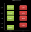
Source:
GPU Café
The entry of a GeForce 9550 GT shows the 9500 GT cannot compete with the HD 4650, a newer price demographic of ~ $129 is shown in that chart that not only indicates prices, but also shows the HD 4650's lead over 9500 GT is so significant that ATI could be comfortable with asking you $20 more than what 9500 GT asks, relative to the range. GPU Café reports that the 9550 GT would be a toned-down (and shrunk) G94, as in the 55 nm G94b, featuring 64 shader processors and a 192-bit memory bus (and presumably, memory configurations such as 384 MB or 768 MB of GDDR3 memory).

58 Comments on NVIDIA Could Ready HD 4670 Competitor
www.xbitlabs.com/news/other/display/20070328080802.html
... has announced 55nm process technology, an optical shrink for its 65nm fabrication process, ... TSMC’s 55nm process technology is a 90% linear-shrink process from 65nm including I/O and analog circuits.
So you are right, G92 to G92b is an optical shrink. That's what 55nm is all about!
PS: your first link is a DDR2 9500GT!
That 9600GT will cost you $109. And if you get the rebate, it will become $79. That can take months. But rebates are temporary. They don't change retail prices on permanent basis.
No changes were made to G92b, they just took the chip and made photocopy that was 40% smaller. That's exactly why I said that G92B is just an optical shrink of G92. G92 on the other hand was much more than a shrink of the G80.
Anyway, forget about everything. It's like talking to a wall or a 3 years old kid who doesn't care about the lesson. :shadedshu
Like i said in my previous post and it comes straight from TSMC's whitepaper:
TSMC’s 55nm process technology is a 90% linear-shrink process from 65nm including I/O and analog circuits.
www.beyond3d.com/content/news/529
I'll quote: TSMC's 55nm process is a 10% linear shrink of 65nm in each dimension, or 19% overall.
80nm was also a 19% shrink, but it did not affect analogue and I/O. This means the scaling wasn't as good as 55nm's in practice.
TSMC's white papers (or any other document for that matter) don't state anything about a reduction in repeaters, so please show me proof. And when we're talking about a reduction of only 19% then power distribution doesn't change that much, specially when both ATI and nVidia increase the frequency of their chips. In their situation power stays on the same level.
Don't mix up theory with facts. And will the admin be so kind and just close this thread. It's been enough.
4870 has 800 'SPU' right? Divide 800 by 5. That's 160. It seems that if ATI decided to slap 300 shaders in their next card and uberclock them, it'd give a MASSIVE boost over the previous generation. Rambling..
This has all probably been said lol..
As you can see except the G80 vs. G92 all of them are pretty close to the theroretical relation. The reason for G80 to fail to the "rule" is that G80 had the video decoding on a sister chip, so it's difficlt to know if the arrangement of the chip is similar. For instance the video decoding "chip" could be just sitting by the side of the GPU in G92 instead of being completely integrated, occupying much more space that would create a gap that could lead to the error. Still the relation is close enough to the theory to "prove" the numbers given at Beyond3D as usual difference were wrong. IMO what they say there applies better to CPUs, because the logic is much smaller in comparison to the rest of the chip.
G94 and RV770 were added to test if number of transistor to chip size relation was consistent enough within the same fab process, so that relation can then be added to the comparison between processes. IMO it's good enough to make a fair guesstimate, and make all other comparisons legitimate.
I'm going to try to make that chart bigger, but other chips are harder to find. Feel free to link sites where transistor count and size of other chips are available.
Cheers.