 / Ryzen 5")
6
Cores
12
Threads
28 W
TDP
3.2 GHz
Frequency
4.9 GHz
Boost
Phoenix2
Codename
Socket FP7
Socket

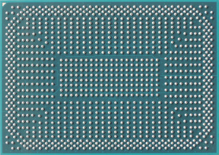
Die Shot

Connectivity
AMD Socket FP7
The AMD Ryzen 5 7545U is a mobile processor with 6 cores, launched in November 2023. It is part of the Ryzen 5 lineup, using the Zen 4 (Phoenix) architecture with Socket FP7. Thanks to AMD Simultaneous Multithreading (SMT) the core-count is effectively doubled, to 12 threads. Ryzen 5 7545U has 16 MB of L3 cache and operates at 3.2 GHz by default, but can boost up to 4.9 GHz, depending on the workload. AMD is building the Ryzen 5 7545U on a 4 nm production process using 20,900 million transistors. The silicon die of the chip is not fabricated at AMD, but at the foundry of TSMC. The multiplier is locked on Ryzen 5 7545U, which limits its overclocking capabilities.
With a TDP of 28 W, the Ryzen 5 7545U consumes only little energy. AMD's processor supports DDR5 memory with a dual-channel interface. The highest officially supported memory speed is 5600 MT/s, but with overclocking (and the right memory modules) you can go even higher. ECC memory is supported, too, which is an important capability for mission-critical systems, to avoid data corruption. For communication with other components in the machine, Ryzen 5 7545U uses a PCI-Express Gen 4 connection. This processor features the Radeon 740M integrated graphics solution.
Hardware virtualization is available on the Ryzen 5 7545U, which greatly improves virtual machine performance. Programs using Advanced Vector Extensions (AVX) will run on this processor, boosting performance for calculation-heavy applications. Besides AVX, AMD has added support for the newer AVX2 and AVX-512 instructions, too.
Physical
| Socket: | AMD Socket FP7 |
|---|---|
| Foundry: | TSMC |
| Process Size: | 4 nm |
| Transistors: | 20,900 million |
| Die Size: | 137 mm² |
| Package: | FP7, FP7r2 |
| tJMax: | 100°C |
Processor
| Market: | Mobile |
|---|---|
| Production Status: | Active |
| Release Date: | Nov 2nd, 2023 |
| Part#: | 100-000000930 (FP7r2) 100-000000929 (FP7) |
Performance
| Frequency: | 3.2 GHz |
|---|---|
| P-Core Base: | 3.7 GHz |
| Turbo Clock: | up to 4.9 GHz |
| E-Core Frequency: |
3 GHz
up to 3.5 GHz |
| Base Clock: | 100 MHz |
| Multiplier: | 32.0x |
| Multiplier Unlocked: | No |
| TDP: | 28 W |
| Configurable TDP: | 15-30 W |
Architecture
| Codename: | Phoenix2 |
|---|---|
| Generation: |
Ryzen 5
(Zen 4 (Phoenix)) |
| Memory Support: | DDR5 |
| Rated Speed: | 5600 MT/s |
| LPDDR5x Speed: | 7500 MT/s |
| Memory Bus: | Dual-channel |
| ECC Memory: | Yes |
| PCI-Express: |
Gen 4, 14 Lanes (CPU only) |
Core Config
| # of Cores: | 6 |
|---|---|
| # of Threads: | 12 |
| Hybrid Cores: | 2 + 4 |
| SMP # CPUs: | 1 |
| Integrated Graphics: | Radeon 740M |
Cache
| Cache L1: | 64 KB (per core) |
|---|---|
| Cache L2: | 1 MB (per core) |
| Cache L3: | 16 MB (shared) |
Features
|
Notes
| Graphics engine boost clock: 2500MHz ECC support on FP7r2 platforms only. |
Jun 12th, 2024 00:06 EDT
change timezone
Latest GPU Drivers
New Forum Posts
- Amd confirms what I already suspected. (27)
- Good Bronze 750w PSU (5)
- What do you mostly use your desktop PC for? (Pick your top 3!) (58)
- AAF Optimus DCH Audio Modded Driver for Windows 10/11 - For ALL HDAUDIO Enumerator Chips (664)
- How Should iGPU be tweaked in comparison to CPU & Cache? (9)
- Last game you purchased? (338)
- ARC "driver issues" turning out to be actually hardware deficiencies - Battlemage reveal (11)
- Need help undervolting MSI GF63 i5 10500h 2.5ghz (1)
- Wrong package power reported by CPU, triggering power throttle (4)
- Can you live with one monitor? ;) (91)
Popular Reviews
- VAXEE Outset AX Wireless (4K) Review
- Intel Lunar Lake Technical Deep Dive - So many Revolutions in One Chip
- Upcoming Hardware Launches 2024 (Updated May 2024)
- Pulsar Xlite V3 Review
- AMD Ryzen 7 7800X3D Review - The Best Gaming CPU
- NZXT H6 Flow RGB Review
- Quick Look: Final UX2000 Wireless Noise Canceling Headphones
- Thermal Grizzly KryoSheet Review - Tested on RX 7900 XTX with 475 W
- ASUS Radeon RX 7900 GRE TUF OC Review
- Ghost of Tsushima Performance Benchmark Review - 35 GPUs Tested
Controversial News Posts
- AMD RDNA 5 a "Clean Sheet" Graphics Architecture, RDNA 4 Merely Corrects a Bug Over RDNA 3 (148)
- NVIDIA RTX 5090 "Blackwell" Founders Edition to Implement the "RTX 4090 Ti" Cinderblock Design (118)
- Possible Specs of NVIDIA GeForce "Blackwell" GPU Lineup Leaked (117)
- Nightmare Fuel for Intel: Arm CEO Predicts Arm will Take Over 50% Windows PC Market-share by 2029 (101)
- AMD Zen 5 Storms into Gaming Desktops with Ryzen 9000 "Granite Ridge" Processors (100)
- Biden Administration to Revive Trump-Era Tariffs on China-made GPUs and Motherboards (95)
- ASRock Innovates First AMD Radeon RX 7000 Graphics Card with 12V-2x6 Power Connector (94)
- AMD Ryzen 9000 Zen 5 Single Thread Performance at 5.80 GHz Found 19% Over Zen 4 (92)