 / Ryzen Embedded")
8
Cores
16
Threads
28 W
TDP
3.3 GHz
Frequency
5.1 GHz
Boost
Hawk Point
Codename
Socket FP8
Socket

Front

Connectivity
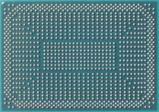
AMD Socket FP8
The AMD Ryzen Embedded 8840U is a mobile processor with 8 cores, launched in April 2024. It is part of the Ryzen Embedded lineup, using the Zen 4 (Hawk Point) architecture with Socket FP8. Thanks to AMD Simultaneous Multithreading (SMT) the core-count is effectively doubled, to 16 threads. Ryzen Embedded 8840U has 16 MB of L3 cache and operates at 3.3 GHz by default, but can boost up to 5.1 GHz, depending on the workload. AMD is making the Ryzen Embedded 8840U on a 4 nm production node using 25,000 million transistors. The silicon die of the chip is not fabricated at AMD, but at the foundry of TSMC. The multiplier is locked on Ryzen Embedded 8840U, which limits its overclocking potential.
With a TDP of 28 W, the Ryzen Embedded 8840U consumes only little energy. AMD's processor supports DDR5 memory with a dual-channel interface. The highest officially supported memory speed is 5600 MT/s. ECC memory is supported, too, which is an important capability for mission-critical systems, to avoid data corruption. For communication with other components in the machine, Ryzen Embedded 8840U uses a PCI-Express Gen 4 connection. This processor features the Radeon 780M integrated graphics solution.
Hardware virtualization is available on the Ryzen Embedded 8840U, which greatly improves virtual machine performance. Programs using Advanced Vector Extensions (AVX) can run on this processor, boosting performance for calculation-heavy applications. Besides AVX, AMD has added support for the newer AVX2 and AVX-512 instructions, too. This processor is equipped with a Neural Processing Unit (NPU) that comes with a performance rating of up to 16 TOPS.
Physical
| Socket: | AMD Socket FP8 |
|---|---|
| Foundry: | TSMC |
| Process Size: | 4 nm |
| Transistors: | 25,000 million |
| Die Size: | 178 mm² |
| Package: | FP8, FP7, FP7r2 |
| tJMax: | 100°C |
Processor
| Market: | Mobile |
|---|---|
| Production Status: | Active |
| Release Date: | Apr 2nd, 2024 |
| Part#: | unknown |
Performance
| Frequency: | 3.3 GHz |
|---|---|
| Turbo Clock: | up to 5.1 GHz |
| Base Clock: | 100 MHz |
| NPU: | Yes / 16 TOPS |
| Multiplier: | 33.0x |
| Multiplier Unlocked: | No |
| TDP: | 28 W |
| Configurable TDP: | 15-30 W |
Architecture
| Codename: | Hawk Point |
|---|---|
| Generation: |
Ryzen Embedded
(Zen 4 (Hawk Point)) |
| Memory Support: | DDR5 |
| LPDDR5x Speed: | 7500 MT/s |
| Rated Speed: | 5600 MT/s |
| Memory Bus: | Dual-channel |
| ECC Memory: | Yes |
| PCI-Express: |
Gen 4, 20 Lanes (CPU only) |
Core Config
| # of Cores: | 8 |
|---|---|
| # of Threads: | 16 |
| SMP # CPUs: | 1 |
| Integrated Graphics: | Radeon 780M |
Cache
| Cache L1: | 64 KB (per core) |
|---|---|
| Cache L2: | 1 MB (per core) |
| Cache L3: | 16 MB (shared) |
Features
|
Notes
| Graphics engine boost clock: 2700MHz |
May 19th, 2025 21:18 EDT
change timezone
Latest GPU Drivers
New Forum Posts
- Ryzen Owners Zen Garden (7791)
- as an AMD fanboy, I gotta say Nvidia's multi frame gen is just lit, even at 1080p (79)
- What's your latest tech purchase? (23837)
- Inland adapters - MHL and IDE/SATA to USB (0)
- Benchmate issues (23)
- Folding Pie and Milestones!! (9542)
- Anyone play WoW in 2004/2005? I was in Nightcrawlers Guild on Durotan server, post your guild/server! (11)
- My rx 580 of 8gb of vram only detect and use 4gb vram (2)
- Vega owners club (571)
- Techpoweups incorrect info for hardware (1)
Popular Reviews
- DOOM: The Dark Ages Performance Benchmark Review - 40 GPUs Tested
- Fractal Design Meshify 3 Ambience Pro RGB Review
- Upcoming Hardware Launches 2025 (Updated May 2025)
- ASRock B850 Steel Legend Wi-Fi Review
- PNY GeForce RTX 5070 Ti Epic-X RGB Plus OC Review
- Clair Obscur: Expedition 33 Performance Benchmark Review - 33 GPUs Tested
- Valkyrie V240 LITE Review
- AMD Ryzen 7 9800X3D Review - The Best Gaming Processor
- Phison PASCARI X200E 6.4 TB Review
- Sapphire Radeon RX 9070 XT Nitro+ Review - Beating NVIDIA
Controversial News Posts
- AMD Radeon RX 9060 XT to Roll Out 8 GB GDDR6 Edition, Despite Rumors (142)
- Microsoft Forces Automatic Windows 11 24H2 Update on Pro and Home PCs (121)
- XFX & Acer Radeon RX 9060 XT Graphics Cards Leaked by Retailers - Starting at "$450" (112)
- Parts of NVIDIA GeForce RTX 50 Series GPU PCB Reach Over 100°C: Report (85)
- AMD "Zen 7" Rumors: Three Core Classes, 2 MB L2, 7 MB V‑Cache, and TSMC A14 Node (79)
- NVIDIA Reportedly Working on GeForce RTX 5080 SUPER 24 GB & RTX 5070 SUPER 18 GB Designs (76)
- NVIDIA Reportedly Limiting Press Access to GeForce RTX 5060 Drivers - Suggesting Late Arrival of Reviews (62)
- Intel Partner Prepares Dual Arc "Battlemage" B580 GPU with 48 GB of VRAM (61)