Report an Error


NVIDIA GeForce GTX 295
- Graphics Processor
- GT200B x2
- Cores
- 240 x2
- TMUs
- 80 x2
- ROPs
- 28 x2
- Memory Size
- 896 MB x2
- Memory Type
- GDDR3
- Bus Width
- 448 bit x2


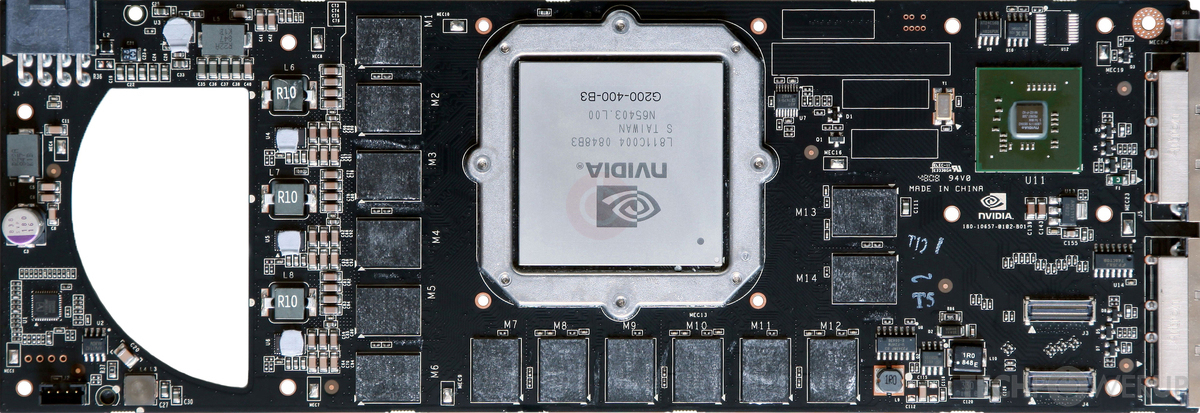
GPU

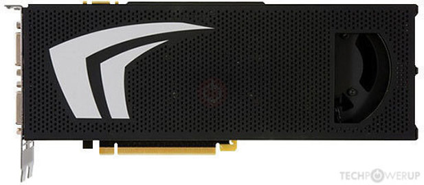
I/O

PCB Front

PCB Back
PCB Front 2

PCB Back 2
Recommended Gaming Resolutions:
- 1600x900
- 1920x1080
- 2560x1440
The GeForce GTX 295 was a high-end graphics card by NVIDIA, launched on January 8th, 2009. Built on the 55 nm process, and based on the GT200B graphics processor, in its G200-400-B3 variant, the card supports DirectX 11.1. Even though it supports DirectX 11, the feature level is only 10_0, which can be problematic with many DirectX 11 & DirectX 12 titles. The GT200B graphics processor is a large chip with a die area of 470 mm² and 1,400 million transistors. GeForce GTX 295 combines two graphics processors to increase performance. It features 240 shading units, 80 texture mapping units, and 28 ROPs, per GPU. NVIDIA has paired 1,792 MB GDDR3 memory with the GeForce GTX 295, which are connected using a 448-bit memory interface per GPU (each GPU manages 896 MB). The GPU is operating at a frequency of 576 MHz, memory is running at 999 MHz.
Being a dual-slot card, the NVIDIA GeForce GTX 295 draws power from 1x 6-pin + 1x 8-pin power connector, with power draw rated at 289 W maximum. Display outputs include: 2x DVI, 1x HDMI. GeForce GTX 295 is connected to the rest of the system using a PCI-Express 2.0 x16 interface. The card's dimensions are 267 mm x 111 mm x 38 mm, and it features a dual-slot cooling solution. Its price at launch was 499 US Dollars.
Being a dual-slot card, the NVIDIA GeForce GTX 295 draws power from 1x 6-pin + 1x 8-pin power connector, with power draw rated at 289 W maximum. Display outputs include: 2x DVI, 1x HDMI. GeForce GTX 295 is connected to the rest of the system using a PCI-Express 2.0 x16 interface. The card's dimensions are 267 mm x 111 mm x 38 mm, and it features a dual-slot cooling solution. Its price at launch was 499 US Dollars.
Graphics Processor
Graphics Processor
Graphics Card
- Release Date
- Jan 8th, 2009
- Generation
- GeForce 200
- Predecessor
- GeForce 9
- Successor
- GeForce 400
- Production
- End-of-life
- Launch Price
- 499 USD
- Bus Interface
- PCIe 2.0 x16
- Reviews
- 74 in our database
Relative Performance
Based on TPU review data: "Performance Summary" at 1920x1080, 4K for 2080 Ti and faster.
Clock Speeds
- GPU Clock
- 576 MHz
- Shader Clock
- 1242 MHz
- Memory Clock
-
999 MHz
1998 Mbps effective
Memory
- Memory Size
- 896 MB
- Memory Type
- GDDR3
- Memory Bus
- 448 bit
- Bandwidth
- 111.9 GB/s
Render Config
- Shading Units
- 240
- TMUs
- 80
- ROPs
- 28
- SM Count
- 30
- L2 Cache
- 224 KB
Theoretical Performance
- Pixel Rate
- 16.13 GPixel/s
- Texture Rate
- 46.08 GTexel/s
- FP32 (float)
- 596.2 GFLOPS
- FP64 (double)
- 74.52 GFLOPS (1:8)
Board Design
- Slot Width
- Dual-slot
- Length
- 267 mm
10.5 inches
- Width
- 111 mm
4.4 inches
- Height
- 38 mm
1.5 inches
- TDP
- 289 W
- Suggested PSU
- 600 W
- Outputs
- 2x DVI
1x HDMI
- Power Connectors
- 1x 6-pin + 1x 8-pin
- Board Number
- P656 SKU 0
Graphics Features
- DirectX
- 11.1 (10_0)
- OpenGL
- 3.3
- OpenCL
- 1.1
- Vulkan
- N/A
- CUDA
- 1.3
- Shader Model
- 4.0
GT200B GPU Notes
| PureVideo HD: VP2 VDPAU: Feature Set A GT200B, commonly printed on the chip package as G200-xxx-Bx is an optical shrink of the G200 core to the newer 55 manufacturing process of TSMC. It helped shrink the core's energy and thermal footprints to a level that even facilitated building a dual-GPU accelerator |
Retail boards based on this design (7)
| Name | GPU Clock | Memory Clock | Other Changes |
|---|---|---|---|
| 604 MHz | 1050 MHz | 2x DVI | |
| 576 MHz | 999 MHz | ||
| 720 MHz | 1080 MHz | 2x DVI | |
| 576 MHz | 999 MHz | ||
| 576 MHz | 999 MHz | ||
| 594 MHz | 1026 MHz | ||
| 576 MHz | 999 MHz |


Apr 28th, 2024 19:01 EDT
change timezone
Latest GPU Drivers
New Forum Posts
- Schede grafiche (2)
- What's your latest tech purchase? (20367)
- Which PSU to take? (40)
- Z790 ACE MAX? (1)
- Looking for recommendations to upgrade the GPU (26)
- Questions about GTX 660 Memory Bus Width (4)
- Your PC ATM (34518)
- best budget freindly 5.1 soundbars in 2024 (0)
- Ryzen Owners Zen Garden (7265)
- New R5 3600 build, memory write speed slow?? (16)
Popular Reviews
- Ugreen NASync DXP4800 Plus Review
- HYTE THICC Q60 240 mm AIO Review
- MOONDROP x Crinacle DUSK In-Ear Monitors Review - The Last 5%
- Upcoming Hardware Launches 2023 (Updated Feb 2024)
- Thermalright Phantom Spirit 120 EVO Review
- AMD Ryzen 7 7800X3D Review - The Best Gaming CPU
- ASUS Radeon RX 7900 GRE TUF OC Review
- FiiO K19 Desktop DAC/Headphone Amplifier Review
- Horizon Forbidden West Performance Benchmark Review - 30 GPUs Tested
- Alienware Pro Wireless Gaming Keyboard Review
Controversial News Posts
- Windows 11 Now Officially Adware as Microsoft Embeds Ads in the Start Menu (139)
- Sony PlayStation 5 Pro Specifications Confirmed, Console Arrives Before Holidays (117)
- NVIDIA Points Intel Raptor Lake CPU Users to Get Help from Intel Amid System Instability Issues (106)
- AMD "Strix Halo" Zen 5 Mobile Processor Pictured: Chiplet-based, Uses 256-bit LPDDR5X (103)
- US Government Wants Nuclear Plants to Offload AI Data Center Expansion (98)
- AMD's RDNA 4 GPUs Could Stick with 18 Gbps GDDR6 Memory (95)
- Developers of Outpost Infinity Siege Recommend Underclocking i9-13900K and i9-14900K for Stability on Machines with RTX 4090 (85)
- Windows 10 Security Updates to Cost $61 After 2025, $427 by 2028 (84)