Report an Error


NVIDIA GeForce 210
- Graphics Processor
- GT218S
- Cores
- 16
- TMUs
- 8
- ROPs
- 4
- Memory Size
- 512 MB
- Memory Type
- DDR3
- Bus Width
- 64 bit

GPU
I/O

Bottom
Back
Recommended Gaming Resolutions:
- 640x480
- 1280x720
- 1366x768
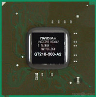
The GeForce 210 was a graphics card by NVIDIA, launched on October 12th, 2009. Built on the 40 nm process, and based on the GT218S graphics processor, in its GT218-300-A2 variant, the card supports DirectX 11.1. Even though it supports DirectX 11, the feature level is only 10_1, which can be problematic with many DirectX 11 & DirectX 12 titles. The GT218S graphics processor is a relatively small chip with a die area of only 57 mm² and 260 million transistors. It features 16 shading units, 8 texture mapping units, and 4 ROPs. NVIDIA has paired 512 MB DDR3 memory with the GeForce 210, which are connected using a 64-bit memory interface. The GPU is operating at a frequency of 520 MHz, memory is running at 400 MHz.
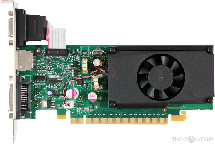
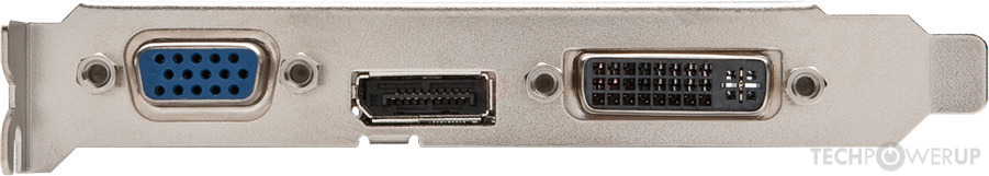
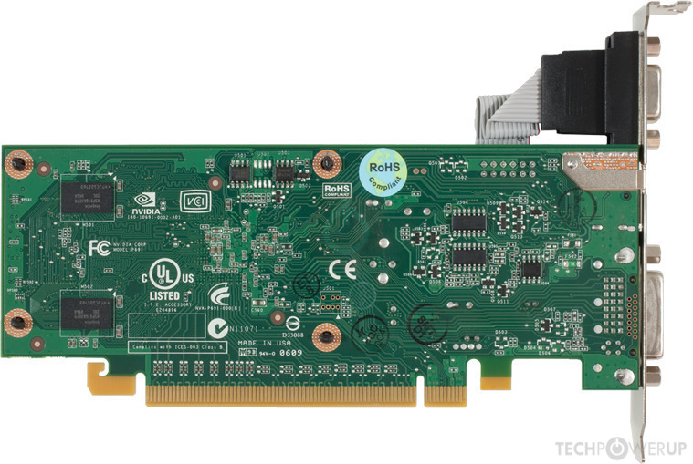
Being a single-slot card, the NVIDIA GeForce 210 does not require any additional power connector, its power draw is rated at 31 W maximum. Display outputs include: 1x DVI, 1x DisplayPort, 1x VGA. GeForce 210 is connected to the rest of the system using a PCI-Express 2.0 x16 interface. The card measures 168 mm in length, and features a single-slot cooling solution.
Being a single-slot card, the NVIDIA GeForce 210 does not require any additional power connector, its power draw is rated at 31 W maximum. Display outputs include: 1x DVI, 1x DisplayPort, 1x VGA. GeForce 210 is connected to the rest of the system using a PCI-Express 2.0 x16 interface. The card measures 168 mm in length, and features a single-slot cooling solution.
Graphics Processor
Graphics Card
- Release Date
- Oct 12th, 2009
- Generation
- GeForce 200
- Predecessor
- GeForce 9
- Successor
- GeForce 400
- Production
- End-of-life
- Bus Interface
- PCIe 2.0 x16
Relative Performance
Based on TPU review data: "Performance Summary" at 1920x1080, 4K for 2080 Ti and faster.
Clock Speeds
- GPU Clock
- 520 MHz
- Shader Clock
- 1230 MHz
- Memory Clock
-
400 MHz
800 Mbps effective
Memory
- Memory Size
- 512 MB
- Memory Type
- DDR3
- Memory Bus
- 64 bit
- Bandwidth
- 6.400 GB/s
Render Config
- Shading Units
- 16
- TMUs
- 8
- ROPs
- 4
- SM Count
- 2
- L2 Cache
- 32 KB
Theoretical Performance
- Pixel Rate
- 2.080 GPixel/s
- Texture Rate
- 4.160 GTexel/s
- FP32 (float)
- 39.36 GFLOPS
Board Design
- Slot Width
- Single-slot
- Length
- 168 mm
6.6 inches
- TDP
- 31 W
- Suggested PSU
- 200 W
- Outputs
- 1x DVI
1x DisplayPort
1x VGA
- Power Connectors
- None
- Board Number
- P691 SKU 3,
P873 SKU 0
Graphics Features
- DirectX
- 11.1 (10_1)
- OpenGL
- 3.3
- OpenCL
- 1.1
- Vulkan
- N/A
- CUDA
- 1.2
- Shader Model
- 4.1
GT218S GPU Notes
| PureVideo HD: VP4 VDPAU: Feature Set C Latest Drivers: Windows 2000: Quadro Release 261.19 Windows XP / Server 2003 x64: GeForce Release 185.81 (Notebooks) GeForce Release 340.52 Quadro Release R319 U2 (321.01) Tesla Release 258.96 Windows Vista: GeForce Release 307.83 (Notebooks) GeForce Release 342.01 Quadro Release R340 U15 (342.01) Tesla Release 258.96 Windows 7 / 8 / 8.1 / 10: GeForce Release 342.01 Quadro Release R340 U15 (342.01) Tesla Release 258.96 |
Retail boards based on this design (13)
| Name | GPU Clock | Memory Clock | Other Changes |
|---|---|---|---|
| 589 MHz | 600 MHz | 1024 MB, 173 mm/6.8 inches, 1x DVI 1x HDMI 1x VGA | |
| 589 MHz | 790 MHz | 178 mm/7 inches, 1x DVI 1x HDMI 1x VGA | |
| 589 MHz | 600 MHz | 1024 MB, 178 mm/7 inches, 1x DVI 1x HDMI 1x VGA | |
| 589 MHz | 667 MHz | 184 mm/7.2 inches, 1x DVI 1x HDMI 1x VGA | |
| 589 MHz | 600 MHz | 1024 MB, 178 mm/7 inches, 1x DVI 1x HDMI 1x VGA | |
| 520 MHz | 600 MHz | 1024 MB, 157 mm/6.2 inches, 1x DVI 1x HDMI 1x VGA | |
| 590 MHz | 550 MHz | 1024 MB, 157 mm/6.2 inches, 1x DVI 1x HDMI 1x VGA | |
| 520 MHz | 600 MHz | 1024 MB, 157 mm/6.2 inches, 1x DVI 1x HDMI 1x VGA | |
| 520 MHz | 600 MHz | 1024 MB, 178 mm/7 inches, 1x DVI 1x HDMI 1x VGA | |
| 520 MHz | 400 MHz | ||
| 589 MHz | 500 MHz | 1024 MB, 150 mm/5.9 inches | |
| 589 MHz | 533 MHz | 1024 MB, 1x DVI 1x HDMI 1x VGA | |
| 500 MHz | 533 MHz | 1024 MB, DDR2, 1x DVI 1x HDMI 1x VGA |


Apr 25th, 2025 06:57 EDT
change timezone
Latest GPU Drivers
New Forum Posts
- Oblivion Remastered (3)
- 5060 Ti 8GB DOA (273)
- Choosing an Internal HDD (22)
- What are you playing? (23463)
- Help getting a mini pc (14)
- How do you calculate the cost of a chip? (5)
- Ghetto Mods (4555)
- Are the 8 GB cards worth it? (181)
- RX 9000 series GPU Owners Club (541)
- I dont understand the phone OS world..... (51)
Popular Reviews
- NVIDIA GeForce RTX 5060 Ti 8 GB Review - So Many Compromises
- Crucial CUDIMM DDR5-6400 128 GB CL52 Review
- Colorful iGame B860M Ultra V20 Review
- ASUS GeForce RTX 5060 Ti TUF OC 16 GB Review
- Upcoming Hardware Launches 2025 (Updated Apr 2025)
- Sapphire Radeon RX 9070 XT Pulse Review
- Sapphire Radeon RX 9070 XT Nitro+ Review - Beating NVIDIA
- ASRock X870E Taichi Lite Review
- AMD Ryzen 7 9800X3D Review - The Best Gaming Processor
- ASUS GeForce RTX 5080 TUF OC Review
Controversial News Posts
- NVIDIA GeForce RTX 5060 Ti 16 GB SKU Likely Launching at $499, According to Supply Chain Leak (182)
- NVIDIA Sends MSRP Numbers to Partners: GeForce RTX 5060 Ti 8 GB at $379, RTX 5060 Ti 16 GB at $429 (127)
- NVIDIA Launches GeForce RTX 5060 Series, Beginning with RTX 5060 Ti This Week (115)
- Nintendo Confirms That Switch 2 Joy-Cons Will Not Utilize Hall Effect Stick Technology (105)
- Nintendo Switch 2 Launches June 5 at $449.99 with New Hardware and Games (99)
- Sony Increases the PS5 Pricing in EMEA and ANZ by Around 25 Percent (84)
- NVIDIA PhysX and Flow Made Fully Open-Source (77)
- Windows Notepad Gets Microsoft Copilot Integration (75)