Report an Error


NVIDIA GeForce GTX 465
- Graphics Processor
- GF100
- Cores
- 352
- TMUs
- 44
- ROPs
- 32
- Memory Size
- 1024 MB
- Memory Type
- GDDR5
- Bus Width
- 256 bit

GPU

PCB Front

PCB Back
Recommended Gaming Resolutions:
- 1366x768
- 1600x900
- 1920x1080
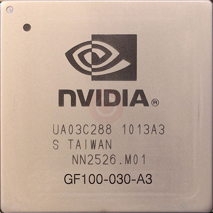
The GeForce GTX 465 was a performance-segment graphics card by NVIDIA, launched on May 31st, 2010. Built on the 40 nm process, and based on the GF100 graphics processor, in its GF100-030-A3 variant, the card supports DirectX 12. Even though it supports DirectX 12, the feature level is only 11_0, which can be problematic with newer DirectX 12 titles. The GF100 graphics processor is a large chip with a die area of 529 mm² and 3,100 million transistors. Unlike the fully unlocked GeForce GTX 480 Core 512, which uses the same GPU but has all 512 shaders enabled, NVIDIA has disabled some shading units on the GeForce GTX 465 to reach the product's target shader count. It features 352 shading units, 44 texture mapping units, and 32 ROPs. NVIDIA has paired 1,024 MB GDDR5 memory with the GeForce GTX 465, which are connected using a 256-bit memory interface. The GPU is operating at a frequency of 608 MHz, memory is running at 802 MHz (3.2 Gbps effective).
Being a dual-slot card, the NVIDIA GeForce GTX 465 draws power from 2x 6-pin power connectors, with power draw rated at 200 W maximum. Display outputs include: 2x DVI, 1x mini-HDMI 1.3a. GeForce GTX 465 is connected to the rest of the system using a PCI-Express 2.0 x16 interface. The card measures 241 mm in length, and features a dual-slot cooling solution. Its price at launch was 279 US Dollars.
Being a dual-slot card, the NVIDIA GeForce GTX 465 draws power from 2x 6-pin power connectors, with power draw rated at 200 W maximum. Display outputs include: 2x DVI, 1x mini-HDMI 1.3a. GeForce GTX 465 is connected to the rest of the system using a PCI-Express 2.0 x16 interface. The card measures 241 mm in length, and features a dual-slot cooling solution. Its price at launch was 279 US Dollars.
Graphics Processor
Graphics Card
- Release Date
- May 31st, 2010
- Generation
- GeForce 400
- Predecessor
- GeForce 200
- Successor
- GeForce 500
- Production
- End-of-life
- Launch Price
- 279 USD
- Bus Interface
- PCIe 2.0 x16
- Reviews
- 37 in our database
Relative Performance
Based on TPU review data: "Performance Summary" at 1920x1080, 4K for 2080 Ti and faster.
Clock Speeds
- GPU Clock
- 608 MHz
- Shader Clock
- 1215 MHz
- Memory Clock
-
802 MHz
3.2 Gbps effective
Memory
- Memory Size
- 1024 MB
- Memory Type
- GDDR5
- Memory Bus
- 256 bit
- Bandwidth
- 102.7 GB/s
Render Config
- Shading Units
- 352
- TMUs
- 44
- ROPs
- 32
- SM Count
- 11
- L1 Cache
- 64 KB (per SM)
- L2 Cache
- 512 KB
Theoretical Performance
- Pixel Rate
- 13.38 GPixel/s
- Texture Rate
- 26.75 GTexel/s
- FP32 (float)
- 855.4 GFLOPS
- FP64 (double)
- 106.9 GFLOPS (1:8)
Board Design
- Slot Width
- Dual-slot
- Length
- 241 mm
9.5 inches
- TDP
- 200 W
- Suggested PSU
- 550 W
- Outputs
- 2x DVI
1x mini-HDMI 1.3a
- Power Connectors
- 2x 6-pin
- Board Number
- P1025 SKU 0008
Graphics Features
- DirectX
- 12 (11_0)
- OpenGL
- 4.6
- OpenCL
- 1.1
- Vulkan
- N/A
- CUDA
- 2.0
- Shader Model
- 5.1
GF100 GPU Notes
| PureVideo HD: VP4 VDPAU: Feature Set C GF100 has 4 GPCs each capable of 8 pixels per clock. This limits complete GPU to 32 pixels per clock and because of that it can't feed all 48 ROPs when they all require data at the same time. Additional ROPs however can be used for MSAA (because it doesn't require additional data from rasterizers, while giving more work to ROPs.) |
Retail boards based on this design (3)
| Name | GPU Clock | Memory Clock | Other Changes |
|---|---|---|---|
| 608 MHz | 802 MHz | 2x DVI 1x HDMI 1x DisplayPort | |
| 608 MHz | 802 MHz | 243 mm/9.6 inches | |
| 608 MHz | 802 MHz |


Apr 28th, 2024 20:56 EDT
change timezone
Latest GPU Drivers
New Forum Posts
- Does charging protection matter? (20)
- Anyone know if Rufus gets around the SSE4.2 issue with Windows 11 24H2? (41)
- Why MS buying all of these Studios is bad for Gaming (17)
- What's an inexpensive AIO product line with a strong pump and low price? (85)
- Your PC ATM (34520)
- Looking for recommendations to upgrade the GPU (27)
- What's your latest tech purchase? (20371)
- New R5 3600 build, memory write speed slow?? (17)
- Ghetto Mods (4326)
- The Official Magic the Gathering card game Rules, Questions, and General Discussion Thread (195)
Popular Reviews
- ASUS GeForce RTX 4070 Ti Super TUF Review
- Ugreen NASync DXP4800 Plus Review
- HYTE THICC Q60 240 mm AIO Review
- MOONDROP x Crinacle DUSK In-Ear Monitors Review - The Last 5%
- Upcoming Hardware Launches 2023 (Updated Feb 2024)
- EVGA GTX 980 Ti SC+ 6 GB Review
- ASUS GeForce RTX 4060 Dual OC Review - The Best RTX 4060
- Noctua NF-A12x25 PWM Fan Review
- Logitech G Pro X Superlight 2 Review - Updated with 4000 Hz Tested
- ASUS GeForce RTX 4090 STRIX OC Review
Controversial News Posts
- Windows 11 Now Officially Adware as Microsoft Embeds Ads in the Start Menu (139)
- Sony PlayStation 5 Pro Specifications Confirmed, Console Arrives Before Holidays (117)
- NVIDIA Points Intel Raptor Lake CPU Users to Get Help from Intel Amid System Instability Issues (106)
- AMD "Strix Halo" Zen 5 Mobile Processor Pictured: Chiplet-based, Uses 256-bit LPDDR5X (103)
- US Government Wants Nuclear Plants to Offload AI Data Center Expansion (98)
- AMD's RDNA 4 GPUs Could Stick with 18 Gbps GDDR6 Memory (95)
- Windows 10 Security Updates to Cost $61 After 2025, $427 by 2028 (84)
- TechPowerUp Hiring: Reviewers Wanted for Motherboards, Laptops, Gaming Handhelds and Prebuilt Desktops (81)