Report an Error


Intel Skylake GT2
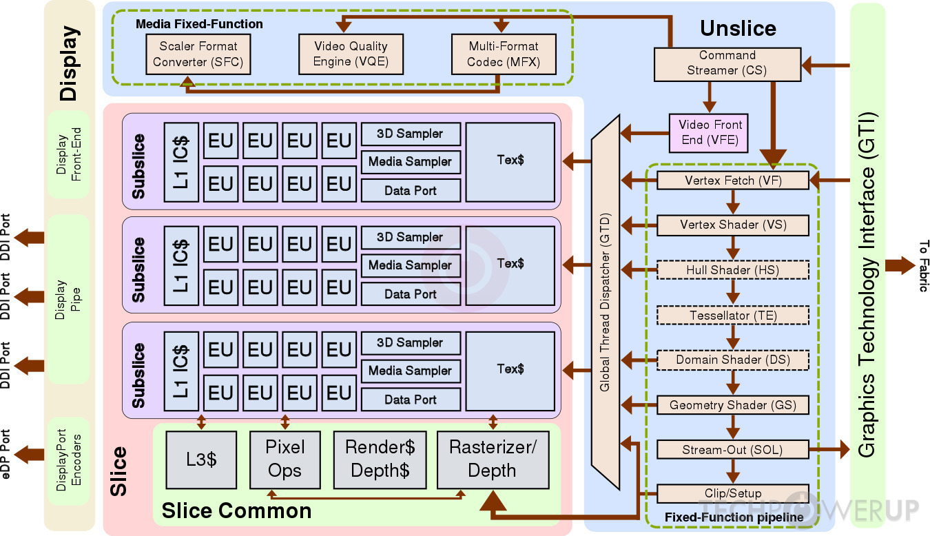
Block Diagram
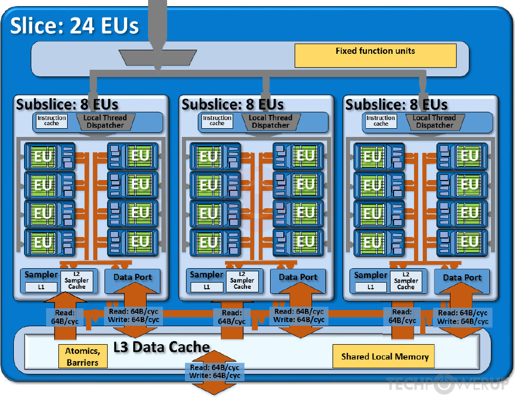
Block Diagram 2
Intel's Skylake GT2 GPU uses the Generation 9.0 architecture and is made using a 14 nm+ production process at Intel. With a die size of 123 mm² it is a small chip. Skylake GT2 supports DirectX 12 (Feature Level 12_1). For GPU compute applications, OpenCL version 3.0 can be used. It features 192 shading units, 24 texture mapping units and 3 ROPs.
Further reading:
Gen 9 Architecture Whitepaper  , Gen 9 Performance Guide
Graphics Processor
- Released
- Sep 1st, 2015
- GPU Name
- Skylake GT2
- Architecture
- Generation 9.0
- Foundry
- Intel
- Process Size
- 14 nm+
- Transistors
- unknown
- Die Size
- 123 mm²
Graphics Features
- DirectX
- 12 (12_1)
- OpenGL
- 4.6
- OpenCL
- 3.0
- Vulkan
- 1.3
- Shader Model
- 6.4
Render Config
- Shading Units
- 192
- TMUs
- 24
- ROPs
- 3
- Execution Units
- 24
- Max. TDP
- 15 W
- Subslice
- 3
All Generation 9.0 GPUs
Intel GPU Architecture History
- 2023 Xe-LPG
- 2022-2023 Generation 12.7
- 2021-2024 Generation 12.5
- 2021-2023 Generation 12.2
- 2020-2021 Generation 12.1
- 2019-2021 Generation 11.0
- 2016-2020 Generation 9.5
- 2015-2016 Generation 9.0
- 2014-2015 Generation 8.0
- 2013 Generation 7.5
- 2012-2013 Generation 7.0
- 2011 Generation 6.0
- 2010-2013 Knights
- 2010 Generation 5.75
- 2008-2010 PowerVR SGX545
- 2008 Generation 5.0
- 2008-2010 PowerVR SGX535
- 2006-2007 Generation 4.0
- 2005-2006 Generation 3.5
- 2004-2005 Generation 3.0
- 2002-2003 Generation 2.0
- 1998 i740
- 1998-2002 Generation 1.0
Graphics cards using the Intel Skylake GT2 GPU
| Name | Chip | Memory | Shaders | TMUs | ROPs | Base Clock | Boost Clock | Memory Clock |
|---|---|---|---|---|---|---|---|---|
| System Shared | 192 | 24 | 3 | 300 MHz | 900 MHz | System Shared | ||
| System Shared | 192 | 24 | 3 | 350 MHz | 950 MHz | System Shared | ||
| System Shared | 192 | 24 | 3 | 350 MHz | 950 MHz | System Shared | ||
| System Shared | 192 | 16 | 3 | 350 MHz | 1000 MHz | System Shared | ||
| System Shared | 192 | 24 | 3 | 300 MHz | 800 MHz | System Shared |


Apr 26th, 2024 22:46 EDT
change timezone
Latest GPU Drivers
New Forum Posts
- Black screens leading to restarts (Event ID 18) on AMD platform since changing graphics card (43)
- FINAL FANTASY XIV: Dawntrail Official Benchmark (73)
- Your PC ATM (34509)
- Rare GPUs / Unreleased GPUs (1877)
- looking to build a new system and im considering asrock brand but i have some doubts/concerns. (15)
- AAF Optimus DCH Audio Modded Driver for Windows 10/11 - For ALL HDAUDIO Enumerator Chips (652)
- Help me identify rx 580 card ? (0)
- Strange system crashes out of nowhere help (9)
- What phone you use as your daily driver? And, a discussion of them. (1494)
- Secure boot already open help (11)
Popular Reviews
- Ugreen NASync DXP4800 Plus Review
- HYTE THICC Q60 240 mm AIO Review
- Quick Look: MOONDROP CHU 2 Budget In-Ear Monitors
- MOONDROP x Crinacle DUSK In-Ear Monitors Review - The Last 5%
- Thermalright Phantom Spirit 120 EVO Review
- Upcoming Hardware Launches 2023 (Updated Feb 2024)
- Alienware Pro Wireless Gaming Keyboard Review
- CeBIT 2008: Akasa Review
- CeBIT 2008: Cyber E Sport Review
- FiiO K19 Desktop DAC/Headphone Amplifier Review
Controversial News Posts
- Windows 11 Now Officially Adware as Microsoft Embeds Ads in the Start Menu (135)
- Sony PlayStation 5 Pro Specifications Confirmed, Console Arrives Before Holidays (117)
- NVIDIA Points Intel Raptor Lake CPU Users to Get Help from Intel Amid System Instability Issues (106)
- AMD "Strix Halo" Zen 5 Mobile Processor Pictured: Chiplet-based, Uses 256-bit LPDDR5X (103)
- US Government Wants Nuclear Plants to Offload AI Data Center Expansion (98)
- AMD's RDNA 4 GPUs Could Stick with 18 Gbps GDDR6 Memory (95)
- Developers of Outpost Infinity Siege Recommend Underclocking i9-13900K and i9-14900K for Stability on Machines with RTX 4090 (85)
- Windows 10 Security Updates to Cost $61 After 2025, $427 by 2028 (84)