Report an Error


NVIDIA GA103

GA103
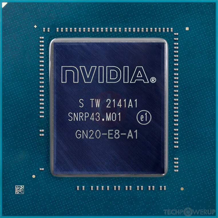
GN20-E8-A1

Block Diagram

SM Diagram
NVIDIA's GA103 GPU uses the Ampere architecture and is made using a 8 nm production process at Samsung. With a die size of 496 mm² and a transistor count of 22,000 million it is a very big chip. GA103 supports DirectX 12 Ultimate (Feature Level 12_2). For GPU compute applications, OpenCL version 3.0 and CUDA 8.6 can be used. Additionally, the DirectX 12 Ultimate capability guarantees support for hardware-raytracing, variable-rate shading and more, in upcoming video games. It features 7680 shading units, 240 texture mapping units and 96 ROPs. Also included are 240 tensor cores which help improve the speed of machine learning applications. The GPU also contains 60 raytracing acceleration cores.
Graphics Processor
- Released
- Jan 25th, 2022
- GPU Name
- GA103
- Codename
- NV173
- Architecture
- Ampere
- Foundry
- Samsung
- Process Size
- 8 nm
- Transistors
- 22,000 million
- Density
- 44.4M / mm²
- Die Size
- 496 mm²
- Package
- BGA-2708
Graphics Features
- DirectX
- 12 Ultimate (12_2)
- OpenGL
- 4.6
- OpenCL
- 3.0
- Vulkan
- 1.3
- CUDA
- 8.6
- Shader Model
- 6.7
- WDDM
- 3.1
- Tensor Cores
- 3rd Gen
- RT Cores
- 2nd Gen
- NVENC
- 7th Gen
- NVDEC
- 5th Gen
- PureVideo HD
- VP11
- VDPAU
- Feature Set K
Render Config
- Shading Units
- 7680
- TMUs
- 240
- ROPs
- 96
- SM Count
- 60
- FP16 Units
- 7680
- FP64 Units
- 120
- INT32 Units
- 3840
- Tensor Cores
- 240
- RT Cores
- 60
- SFUs
- 960
- TPCs
- 30
- GPCs
- 6
- L1 Cache
- 128 KB per SM
- L2 Cache
- 4096 KB
- Max. TDP
- 200 W
All Ampere GPUs
NVIDIA GPU Architecture History
- 2023 Hopper
- 2022-2024 Ada Lovelace
- 2020-2024 Ampere
- 2018-2022 Turing
- 2017-2020 Volta
- 2016-2021 Pascal
- 2014-2019 Maxwell 2.0
- 2014-2017 Maxwell
- 2013-2015 Kepler 2.0
- 2012-2018 Kepler
- 2010-2016 Fermi 2.0
- 2010-2013 VLIW Vec4
- 2010-2016 Fermi
- 2007-2013 Tesla 2.0
- 2006-2010 Tesla
- 2003-2013 Curie
- 2003-2005 Rankine
- 2001-2003 Kelvin
- 1999-2005 Celsius
- 1998-2000 Fahrenheit
Graphics cards using the NVIDIA GA103 GPU
| Name | Chip | Memory | Shaders | TMUs | ROPs | Base Clock | Boost Clock | Memory Clock |
|---|---|---|---|---|---|---|---|---|
| GN20-E8-A1 | 16 GB | 7424 | 232 | 96 | 810 MHz | 1260 MHz | 2000 MHz | |
| GN20-E8-A1 | 16 GB | 7424 | 232 | 96 | 585 MHz | 1125 MHz | 1500 MHz | |
| GA103-200-A1 | 8 GB | 4864 | 152 | 80 | 1410 MHz | 1665 MHz | 1750 MHz | |
| 16 GB | 7424 | 232 | 96 | 975 MHz | 1500 MHz | 2000 MHz | ||
| 16 GB | 7424 | 232 | 96 | 585 MHz | 1260 MHz | 1750 MHz |

GA103 GPU Notes
| Ray Tracing Cores: 2nd Gen Tensor Cores: 3rd Gen NVENC: 7th Gen NVDEC: 5th Gen PureVideo HD: VP11 VDPAU: Feature Set K |
Apr 26th, 2024 02:51 EDT
change timezone
Latest GPU Drivers
New Forum Posts
- What's your latest tech purchase? (20342)
- What phone you use as your daily driver? And, a discussion of them. (1483)
- Best SSD for system drive (81)
- AMD RX 7000 series GPU Owners' Club (1087)
- im new to throttelstop and i think i messed it up by copying others any hints would be very much aprreciated (3)
- Horizontal black lines popping up on my screen? (4)
- Which new games will you be buying? (316)
- Alphacool CORE 1 CPU block - bulging with danger of splitting? (20)
- Black screen after muting (5)
- What are you playing? (20530)
Popular Reviews
- Fractal Design Terra Review
- Thermalright Phantom Spirit 120 EVO Review
- Corsair 2000D Airflow Review
- ASUS GeForce RTX 4090 STRIX OC Review
- NVIDIA GeForce RTX 4090 Founders Edition Review - Impressive Performance
- ASUS GeForce RTX 4090 Matrix Platinum Review - The RTX 4090 Ti
- MSI GeForce RTX 4090 Suprim X Review
- Gigabyte GeForce RTX 4090 Gaming OC Review
- MSI GeForce RTX 4090 Gaming X Trio Review
- MSI GeForce RTX 4090 Suprim Liquid X Review
Controversial News Posts
- Sony PlayStation 5 Pro Specifications Confirmed, Console Arrives Before Holidays (117)
- Windows 11 Now Officially Adware as Microsoft Embeds Ads in the Start Menu (112)
- NVIDIA Points Intel Raptor Lake CPU Users to Get Help from Intel Amid System Instability Issues (106)
- AMD "Strix Halo" Zen 5 Mobile Processor Pictured: Chiplet-based, Uses 256-bit LPDDR5X (101)
- US Government Wants Nuclear Plants to Offload AI Data Center Expansion (98)
- AMD's RDNA 4 GPUs Could Stick with 18 Gbps GDDR6 Memory (88)
- Developers of Outpost Infinity Siege Recommend Underclocking i9-13900K and i9-14900K for Stability on Machines with RTX 4090 (85)
- Windows 10 Security Updates to Cost $61 After 2025, $427 by 2028 (84)