Report an Error


ATI Radeon X1600 PRO
- Graphics Processor
- RV530
- Pixel Shaders
- 12
- Vertex Shaders
- 5
- TMUs
- 4
- ROPs
- 4
- Memory Size
- 256 MB
- Memory Type
- GDDR3
- Bus Width
- 128 bit
GPU
Recommended Gaming Resolutions:
- 640x480
- 1280x720
- 1366x768
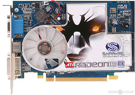
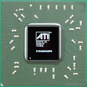
The Radeon X1600 PRO was a performance-segment graphics card by ATI, launched on October 1st, 2005. Built on the 90 nm process, and based on the RV530 graphics processor, in its RV530 PRO variant, the card supports DirectX 9.0c. Since Radeon X1600 PRO does not support DirectX 11 or DirectX 12, it might not be able to run all the latest games. The RV530 graphics processor is an average sized chip with a die area of 150 mm² and 157 million transistors. It features 12 pixel shaders and 5 vertex shaders, 4 texture mapping units, and 4 ROPs. Due to the lack of unified shaders you will not be able to run recent games at all (which require unified shader/DX10+ support). ATI has paired 256 MB GDDR3 memory with the Radeon X1600 PRO, which are connected using a 128-bit memory interface. The GPU is operating at a frequency of 500 MHz, memory is running at 390 MHz.
Being a single-slot card, the ATI Radeon X1600 PRO does not require any additional power connector, its power draw is rated at 41 W maximum. Display outputs include: 1x DVI, 1x VGA, 1x S-Video. Radeon X1600 PRO is connected to the rest of the system using a PCI-Express 1.0 x16 interface. Its price at launch was 199 US Dollars.
Being a single-slot card, the ATI Radeon X1600 PRO does not require any additional power connector, its power draw is rated at 41 W maximum. Display outputs include: 1x DVI, 1x VGA, 1x S-Video. Radeon X1600 PRO is connected to the rest of the system using a PCI-Express 1.0 x16 interface. Its price at launch was 199 US Dollars.
Graphics Processor
- GPU Name
- RV530
- GPU Variant
-
RV530 PRO
(215CADAKA24FG)
- Architecture
- Ultra-Threaded SE
- Foundry
- TSMC
- Process Size
- 90 nm
- Transistors
- 157 million
- Density
- 1.0M / mm²
- Die Size
- 150 mm²
Graphics Card
- Release Date
- Oct 1st, 2005
- Generation
-
Radeon R500 PCIe
(X1600)
- Predecessor
- Radeon R400 PCIe
- Successor
- Radeon R600
- Production
- End-of-life
- Launch Price
- 199 USD
- Bus Interface
- PCIe 1.0 x16
- Reviews
- 64 in our database
Clock Speeds
- GPU Clock
- 500 MHz
- Memory Clock
-
390 MHz
780 Mbps effective
Memory
- Memory Size
- 256 MB
- Memory Type
- GDDR3
- Memory Bus
- 128 bit
- Bandwidth
- 12.48 GB/s
Render Config
- Pixel Shaders
- 12
- Vertex Shaders
- 5
- TMUs
- 4
- ROPs
- 4
Theoretical Performance
- Pixel Rate
- 2.000 GPixel/s
- Vertex Rate
- 625.0 MVertices/s
- Texture Rate
- 2.000 GTexel/s
Board Design
- Slot Width
- Single-slot
- TDP
- 41 W
- Suggested PSU
- 200 W
- Outputs
- 1x DVI
1x VGA
1x S-Video
- Power Connectors
- None
- Board Number
- A676
Graphics Features
- DirectX
- 9.0c (9_3)
- OpenGL
- 2.1
- OpenCL
- N/A
- Vulkan
- N/A
- Shader Model
- 3.0
RV530 GPU Notes
| Mobile Variant: M56 / M66 Codename: Jinn Graphics/Compute: GFX2 Display Core Engine: 1.0 Avivo Video Programmable pixel&vertex pipelines RV530 Chip Numbers: RV530 XT ES (215CACAKA13FG) |
Retail boards based on this design (6)
| Name | GPU Clock | Memory Clock | Other Changes |
|---|---|---|---|
| 500 MHz | 390 MHz | ||
| 500 MHz | 390 MHz | 512 MB | |
| 500 MHz | 390 MHz | 2x DVI 1x S-Video | |
| 500 MHz | 390 MHz | 128 MB, 1x HDMI 1x VGA | |
| 500 MHz | 390 MHz | 1x HDMI 1x VGA | |
| 500 MHz | 390 MHz |


Apr 27th, 2024 20:30 EDT
change timezone
Latest GPU Drivers
New Forum Posts
- On ACER V3-772G GDDR5 laptop no display (5)
- Ryzen Owners Zen Garden (7255)
- Anyone know if Rufus gets around the SSE4.2 issue with Windows 11 24H2? (28)
- RTX 3080 and RX 6800XT video/graphics cards (4)
- Your PC ATM (34514)
- Best SSD for system drive (107)
- Core PL1 + GPU PL1 + Ring EDP OTHER (11)
- Which air cooler for a ryzen 9 5900x (168)
- Black screens leading to restarts (Event ID 18) on AMD platform since changing graphics card (45)
- Usb 3.2 and usbc speeds became very slow (6)
Popular Reviews
- Ugreen NASync DXP4800 Plus Review
- HYTE THICC Q60 240 mm AIO Review
- Palit GeForce RTX 4090 GameRock OC Review
- MSI GeForce RTX 4090 Suprim X Review
- Zotac GeForce RTX 4090 Amp Extreme Airo Review
- Colorful GeForce RTX 4090 Vulcan OC-V Review
- ASUS GeForce RTX 4090 Matrix Platinum Review - The RTX 4090 Ti
- ASUS GeForce RTX 4090 STRIX OC Review
- Gigabyte GeForce RTX 4090 Gaming OC Review
- MSI GeForce RTX 4090 Suprim Liquid X Review
Controversial News Posts
- Windows 11 Now Officially Adware as Microsoft Embeds Ads in the Start Menu (139)
- Sony PlayStation 5 Pro Specifications Confirmed, Console Arrives Before Holidays (117)
- NVIDIA Points Intel Raptor Lake CPU Users to Get Help from Intel Amid System Instability Issues (106)
- AMD "Strix Halo" Zen 5 Mobile Processor Pictured: Chiplet-based, Uses 256-bit LPDDR5X (103)
- US Government Wants Nuclear Plants to Offload AI Data Center Expansion (98)
- AMD's RDNA 4 GPUs Could Stick with 18 Gbps GDDR6 Memory (95)
- Developers of Outpost Infinity Siege Recommend Underclocking i9-13900K and i9-14900K for Stability on Machines with RTX 4090 (85)
- Windows 10 Security Updates to Cost $61 After 2025, $427 by 2028 (84)