Report an Error


NVIDIA GeForce GT 610
- Graphics Processor
- GF119S
- Cores
- 48
- TMUs
- 8
- ROPs
- 4
- Memory Size
- 1024 MB
- Memory Type
- DDR3
- Bus Width
- 64 bit

GPU
Recommended Gaming Resolutions:
- 640x480
- 1280x720
- 1366x768
The GeForce GT 610 was a graphics card by NVIDIA, launched on April 2nd, 2012. Built on the 40 nm process, and based on the GF119S graphics processor, in its GF119-300-A1 variant, the card supports DirectX 12. Even though it supports DirectX 12, the feature level is only 11_0, which can be problematic with newer DirectX 12 titles. The GF119S graphics processor is a relatively small chip with a die area of only 79 mm² and 292 million transistors. It features 48 shading units, 8 texture mapping units, and 4 ROPs. NVIDIA has paired 1,024 MB DDR3 memory with the GeForce GT 610, which are connected using a 64-bit memory interface. The GPU is operating at a frequency of 810 MHz, memory is running at 898 MHz.
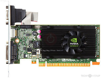
Being a single-slot card, the NVIDIA GeForce GT 610 does not require any additional power connector, its power draw is rated at 29 W maximum. Display outputs include: 1x DVI, 1x HDMI 1.3a, 1x VGA. GeForce GT 610 is connected to the rest of the system using a PCI-Express 2.0 x16 interface. The card measures 145 mm in length, and features a single-slot cooling solution.
Being a single-slot card, the NVIDIA GeForce GT 610 does not require any additional power connector, its power draw is rated at 29 W maximum. Display outputs include: 1x DVI, 1x HDMI 1.3a, 1x VGA. GeForce GT 610 is connected to the rest of the system using a PCI-Express 2.0 x16 interface. The card measures 145 mm in length, and features a single-slot cooling solution.
Graphics Processor
Graphics Card
- Release Date
- Apr 2nd, 2012
- Generation
- GeForce 600
- Predecessor
- GeForce 500
- Successor
- GeForce 700
- Production
- End-of-life
- Bus Interface
- PCIe 2.0 x16
Relative Performance
Based on TPU review data: "Performance Summary" at 1920x1080, 4K for RTX 3080 and faster.
Performance estimated based on architecture, shader count and clocks.
Clock Speeds
- GPU Clock
- 810 MHz
- Shader Clock
- 1620 MHz
- Memory Clock
-
898 MHz
1796 Mbps effective
Memory
- Memory Size
- 1024 MB
- Memory Type
- DDR3
- Memory Bus
- 64 bit
- Bandwidth
- 14.37 GB/s
Render Config
- Shading Units
- 48
- TMUs
- 8
- ROPs
- 4
- SM Count
- 1
- L1 Cache
- 64 KB (per SM)
- L2 Cache
- 128 KB
Theoretical Performance
- Pixel Rate
- 1.620 GPixel/s
- Texture Rate
- 6.480 GTexel/s
- FP32 (float)
- 155.5 GFLOPS
- FP64 (double)
- 12.96 GFLOPS (1:12)
Board Design
- Slot Width
- Single-slot
- Length
- 145 mm
5.7 inches
- TDP
- 29 W
- Suggested PSU
- 200 W
- Outputs
- 1x DVI
1x HDMI 1.3a
1x VGA
- Power Connectors
- None
- Board Number
- P1310 SKU 1,
P1310 SKU 4
Graphics Features
- DirectX
- 12 (11_0)
- OpenGL
- 4.6
- OpenCL
- 1.1
- Vulkan
- N/A
- CUDA
- 2.1
- Shader Model
- 5.1
GF119S GPU Notes
| PureVideo HD: VP5 VDPAU: Feature Set D Latest Drivers: Windows XP / Server 2003 x64: GeForce Release 368.81 Quadro Release R319 U2 (321.01) Windows Vista: GeForce Release 365.19 Quadro Release R346 U7 (348.40) / R352 BETA (352.86) Windows 7 / 8 / 8.1 / 10: GeForce Release 391.35 Quadro Release R390 U9 (392.37) |
Retail boards based on this design (39)
| Name | GPU Clock | Memory Clock | Other Changes |
|---|---|---|---|
| 810 MHz | 600 MHz | 165 mm/6.5 inches | |
| 810 MHz | 600 MHz | 185 mm/7.3 inches | |
| 810 MHz | 600 MHz | 2 GB, 185 mm/7.3 inches | |
| 810 MHz | 600 MHz | 2 GB, 185 mm/7.3 inches | |
| 810 MHz | 500 MHz | 2 GB | |
| 810 MHz | 500 MHz | 2x DVI 1x mini-HDMI | |
| 810 MHz | 500 MHz | 2 GB, 2x DVI 1x mini-HDMI | |
| 810 MHz | 500 MHz | ||
| 810 MHz | 500 MHz | 2 GB | |
| 830 MHz | 500 MHz | 2 GB, 2x DVI 1x mini-HDMI | |
| 810 MHz | 535 MHz | 168 mm/6.6 inches | |
| 810 MHz | 500 MHz | 2 GB, 1x DVI 1x VGA | |
| 810 MHz | 500 MHz | 2x DMS-59 | |
| 810 MHz | 667 MHz | ||
| 810 MHz | 600 MHz | ||
| 810 MHz | 500 MHz | 2x DMS-59 | |
| 810 MHz | 533 MHz | ||
| 810 MHz | 650 MHz | 2 GB | |
| 810 MHz | 750 MHz | 152 mm/6 inches, 1x DVI 1x HDMI 1x VGA | |
| 810 MHz | 500 MHz | 144 mm/5.7 inches | |
| 810 MHz | 500 MHz | 2 GB, 144 mm/5.7 inches | |
| 810 MHz | 500 MHz | 147 mm/5.8 inches | |
| 810 MHz | 500 MHz | 2 GB, 147 mm/5.8 inches | |
| 810 MHz | 667 MHz | 167 mm/6.6 inches | |
| 550 MHz | 500 MHz | 160 mm/6.3 inches | |
| 810 MHz | 667 MHz | 2 GB, 167 mm/6.6 inches | |
| 810 MHz | 535 MHz | ||
| 810 MHz | 535 MHz | 2 GB | |
| 810 MHz | 535 MHz | ||
| 810 MHz | 500 MHz | ||
| 810 MHz | 533 MHz | ||
| 810 MHz | 898 MHz | 2 GB | |
| 810 MHz | 500 MHz | 2 GB | |
| 810 MHz | 500 MHz | ||
| 810 MHz | 500 MHz | ||
| 810 MHz | 533 MHz | 2 GB | |
| 810 MHz | 667 MHz | ||
| 810 MHz | 533 MHz | 2 GB | |
| 810 MHz | 533 MHz | GDDR3, Dual-slot, 2x DVI 1x HDMI |


Jul 25th, 2025 08:40 CDT
change timezone
Latest GPU Drivers
New Forum Posts
- Diablo 4 paragon points (8)
- What would you buy? (103)
- Corsair RM850x (2021) 12V Rail Dropping — Causing Crashes While Gaming (22)
- How to get free Windows 10 security updates through October 2026: Two ways (12)
- R9 7900X - 5070Ti - Lags / Stuttering (33)
- Solidigm NVMe Custom Modded Driver for All NVMe Brands SSDs & Any NVMe SSDs (236)
- A Final Fantasy IX Reminiscence - My love letter and homage to one of the best stories ever told (127)
- AI Job Losses: let's count the losses up, total losses to AI so far 94,000 and counting (67)
- What's your latest tech purchase? (24364)
- TechPowerUp Screenshot Thread (MASSIVE 56K WARNING) (4278)
Popular Reviews
- Noctua NF-A12x25 G2 PWM Fan Review
- MSI MPG B850I Edge Ti Wi-Fi Review
- UPERFECT UMax 24 Review
- Cougar OmnyX Review
- TerraMaster F4-424 Max Review - The fastest NAS we've tested so far
- VAXEE XE V2 Wireless Review
- Sharkoon OfficePal C10 Review - Affordable and Decent
- Thermal Grizzly WireView Pro Review
- Upcoming Hardware Launches 2025 (Updated May 2025)
- Sapphire Radeon RX 9060 XT Pulse OC 16 GB Review - An Excellent Choice
TPU on YouTube
Controversial News Posts
- Some Intel Nova Lake CPUs Rumored to Challenge AMD's 3D V-Cache in Desktop Gaming (140)
- AMD Radeon RX 9070 XT Gains 9% Performance at 1440p with Latest Driver, Beats RTX 5070 Ti (131)
- AMD's Upcoming UDNA / RDNA 5 GPU Could Feature 96 CUs and 384-bit Memory Bus (121)
- NVIDIA GeForce RTX 5080 SUPER Could Feature 24 GB Memory, Increased Power Limits (115)
- NVIDIA DLSS Transformer Cuts VRAM Usage by 20% (99)
- AMD Sampling Next-Gen Ryzen Desktop "Medusa Ridge," Sees Incremental IPC Upgrade, New cIOD (97)
- NVIDIA Becomes First Company Ever to Hit $4 Trillion Market-Cap (94)
- Windows 12 Delayed as Microsoft Prepares Windows 11 25H2 Update (92)