News Posts matching #16 nm

Return to Keyword Browsing

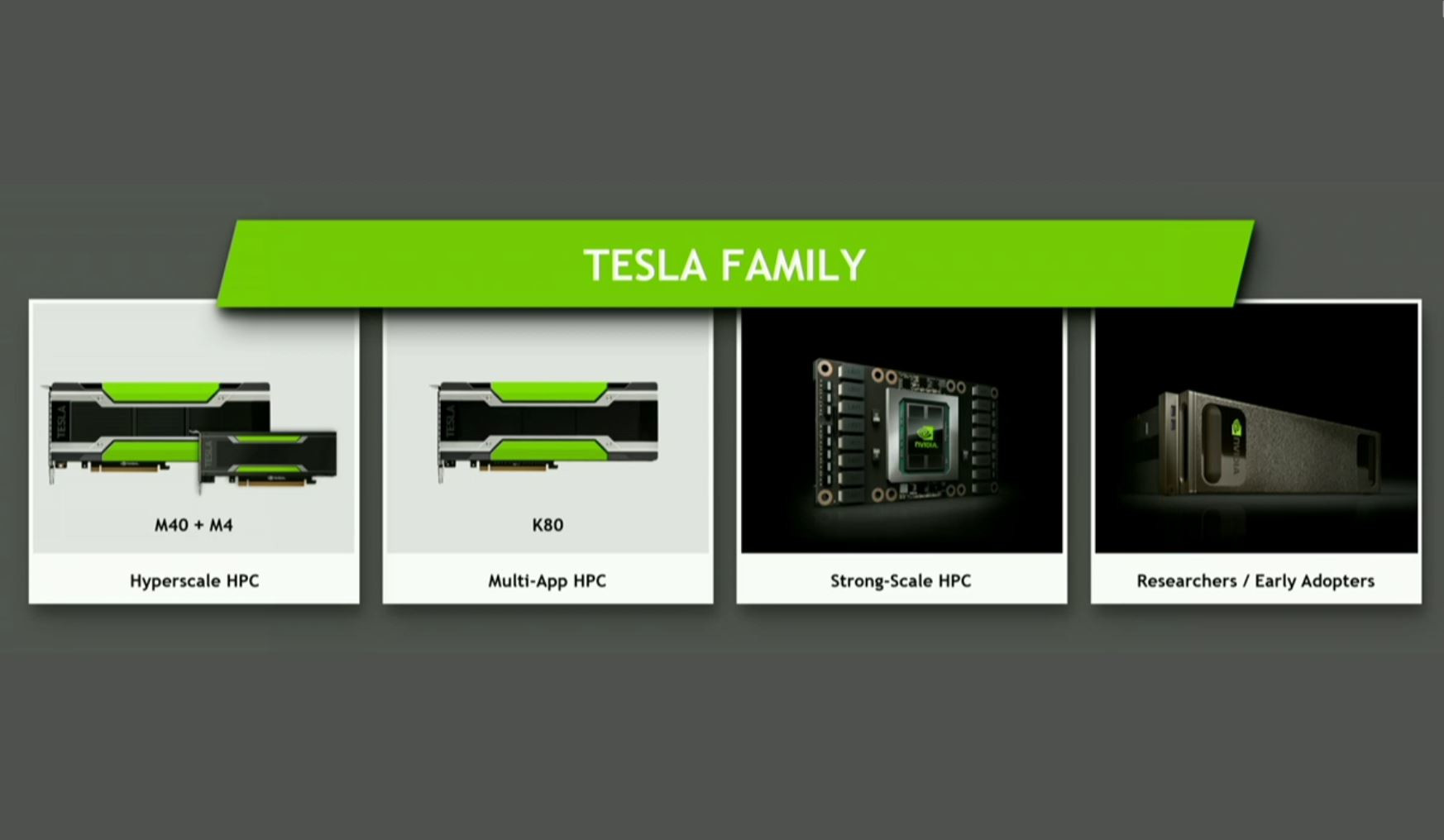
AMD Radeon R9 480 (non-X) Performs Close to R9 390X

In all the 16 nm NVIDIA "Pascal" GPU fervor, it would be foolish to ignore AMD's first "Polaris" GPUs, built on the more advanced 14 nm process. Hot on the heels of reports that a fully-equipped "Ellesmere" GPU based Radeon R9 490 performs close to NVIDIA's GeForce GTX 980 Ti (and AMD's own R9 Fury X), with nearly half its power-draw, new numbers from an early GFXBench run suggests that its cut-down R9 480 (non-X) sibling performs close to the Radeon R9 390X. The R9 480 succeeds the currently-$200 R9 380, and its prospect of offering performance rivaling the $400 R9 390X at half its power-draw appears to meet AMD's "generational leap" claims for the "Polaris" architecture. Similarly, the R9 490, based on a better-endowed "Ellesmere" chip, offering performance rivaling current $600 GPUs at a $350-ish price-point (succeeding the R9 390), appears to meet expectations of a generation leap.

TSMC to Begin 7 nm Trial Production in 2017

Taiwan's premier semiconductor foundry TSMC could begin 7 nanometer (nm) trial production in as early as the first half of 2017. Co-CEO Mark Liu, speaking at the company's investor-meet held earlier this month, stated that TSMC is currently engaging with over 20 companies on 7 nm development, with over 15 tape-outs within 2017, leading up to volume-production by early-2018. In the run-up to 7 nm, the company is also developing a 10 nm node for lower-powered devices (eg: mobile baseband). The company has already begun tape-outs of 10 nm chips in Q1-2016. TSMC is currently handling volume-production of 16 nm FinFET Plus chips.

NVIDIA Readies Three GP104 "Pascal" Based SKUs for June 2016

NVIDIA is reportedly giving final touches to no less than three SKUs based on the 16 nm GP104 silicon, to launch some time this June. The ASIC markings for the chips that drive these SKUs are "GP104-400-A1," "GP104-200-A1" and "GP104-150-A1." If you recall, NVIDIA last reserved the "-400-A1" markings for the GeForce GTX 980 (GM204-400-A1), and the "-200-A1" for the GTX 970 (GM204-200-A1).

The GP104-150-A1 is a mystery ASIC. Either it will drive a more affordable third desktop SKU based on the GP104, or could signify a mobile SKU. The company plans to launch the products based on the GP104-400-A1 and GP104-200-A1, logical successors to the GeForce GTX 980 and GTX 970, in early June. The GP104-150-A1, on the other hand, could see the light of the day in mid-June.

NVIDIA Unveils the Tesla P100 HPC Board based on "Pascal" Architecture

NVIDIA unveiled the Tesla P100, the first product based on the company's "Pascal" GPU architecture. At its core is a swanky new multi-chip module, similar in its essential layout to the AMD "Fiji." A 15 billion-transistor GPU die sits on top of a silicon wafer, through which a 4096-bit wide HBM2 memory interface wires it to four 3D HBM2 stacks; and with the wafer sitting on the fiberglass substrate that's rooted into the PCB over a ball-grid array. With the GPU die, wafer, and memory dies put together, this package has a cumulative transistor count of 150 billion transistors. The GPU die is built on the 16 nm FinFET process, and is 600 mm² in area.

The P100 sits on top of a space-efficient PCB that looks less like a video card, and more like a compact module that can be tucked away into ultra-high density supercomputing cluster boxes, such as the new NVIDIA DGX-1. The P100 offers a double-precision (FP64) compute performance of 5.3 TFLOP/s, FP32 performance of 10.6 TFLOP/s, and FP16 performance of a whopping 21.2 TFLOP/s. The chip has registers as big as 14.2 MB, and an L2 cache of 4 MB. In addition to PCI-Express, each P100 chip will be equipped with NVLink, and in-house developed high-bandwidth interconnect by NVIDIA, with bandwidths as high as 80 GB/s per direction, 160 GB/s both directions. This allows extremely high-bandwidth paths between GPUs, so they could share memory and work more like single-GPUs. The P100 is already in volume production, with its target customers already having bought it all the way up to its OEM channel availability some time in Q1-2017.

NVIDIA's Next Flagship Graphics Cards will be the GeForce X80 Series

With the GeForce GTX 900 series, NVIDIA has exhausted its GeForce GTX nomenclature, according to a sensational scoop from the rumor mill. Instead of going with the GTX 1000 series that has one digit too many, the company is turning the page on the GeForce GTX brand altogether. The company's next-generation high-end graphics card series will be the GeForce X80 series. Based on the performance-segment "GP104" and high-end "GP100" chips, the GeForce X80 series will consist of the performance-segment GeForce X80, the high-end GeForce X80 Ti, and the enthusiast-segment GeForce X80 TITAN.

Based on the "Pascal" architecture, the GP104 silicon is expected to feature as many as 4,096 CUDA cores. It will also feature 256 TMUs, 128 ROPs, and a GDDR5X memory interface, with 384 GB/s memory bandwidth. 6 GB could be the standard memory amount. Its texture- and pixel-fillrates are rated to be 33% higher than those of the GM200-based GeForce GTX TITAN X. The GP104 chip will be built on the 16 nm FinFET process. The TDP of this chip is rated at 175W.

NVIDIA "GP104" Silicon to Feature GDDR5X Memory Interface

It looks like NVIDIA's next GPU architecture launch will play out much like its previous two generations - launching the second biggest chip first, as a well-priced "enthusiast" SKU that outperforms the previous-generation enthusiast product, and launching the biggest chip later, as the high-end enthusiast product. The second-biggest chip based on NVIDIA's upcoming "Pascal" architecture, the "GP104," which could let NVIDIA win crucial $550 and $350 price-points, will be a lean machine. NVIDIA will design the chip to keep manufacturing costs low enough to score big in price-performance, and a potential price-war with AMD.

As part of its efforts to keep GP104 as cost-effective as possible, NVIDIA could give exotic new tech such as HBM2 memory a skip, and go with GDDR5X. Implementing GDDR5X could be straightforward and cost-effective for NVIDIA, given that it's implemented the nearly-identical GDDR5 standard on three previous generations. The new standard will double densities, and one could expect NVIDIA to build its GP104-based products with 8 GB of standard memory amounts. GDDR5X breathed a new lease of life to GDDR5, which had seen its clock speeds plateau around 7 Gbps/pin. The new standard could come in speeds of up to 10 Gbps at first, and eventually 12 Gbps and 14 Gbps. NVIDIA could reserve HBM2 for its biggest "Pascal" chip, on which it could launch its next TITAN product.

NVIDIA to Unveil "Pascal" at the 2016 Computex

NVIDIA is reportedly planning to unveil its next-generation GeForce GTX "Pascal" GPUs at the 2016 Computex show, in Taipei, scheduled for early-June. This unveiling doesn't necessarily mean market availability. SweClockers reports that problems, particularly related to NVIDIA supplier TSMC getting its 16 nm FinFET node up to speed, especially following the recent Taiwan earthquake, could delay market available to late- or even post-Summer. It remains to be seen if the "Pascal" architecture debuts as an all-mighty "GP100" chip, or a smaller, performance-segment "GP104" that will be peddled as enthusiast-segment over being faster than the current big-chip, the GM200. NVIDIA's next generation GeForce nomenclature will also be particularly interesting to look out for, given that the current lineup is already at the GTX 900 series.

TSMC to Launch its 5 nm Fab by 2020

Taiwan's premier semiconductor foundry, TSMC, announced that it is on track to begin production of chips on its 7 nanometer silicon fab process by the first half of 2018. The company also announced that production on an even newer 5 nanometer process should commence two years later, in 2020. The company has currently cleared all decks for mass-production of chips on its 16 nm FFC (FinFET compact) node, with the company hoping to grab over 70% of the worldwide 14/16 nm production market-share by the end of 2016.

NVIDIA GP100 Silicon Moves to Testing Phase

NVIDIA's next-generation flagship graphics processor, codenamed "GP100," has reportedly graduated to testing phase. That is when a limited batch of completed chips are sent from the foundry partner to NVIDIA for testing and evaluation. The chips tripped speed-traps on changeover airports, on their way to NVIDIA. 3DCenter.org predicts that the GP100, based on the company's "Pascal" GPU architecture, will feature no less than 17 billion transistors, and will be built on the 16 nm FinFET+ node at TSMC. The GP100 will feature an HBM2 memory interface. HBM2 allows you to cram up to 32 GB of memory. The flagship product based on GP100 could feature about 16 GB of memory. NVIDIA's design goal could be to squeeze out anywhere between 60-90% higher performance than the current-generation flagship GTX TITAN-X.

NVIDIA "Pascal" GPUs to be Built on 16 nm TSMC FinFET Node

NVIDIA's next-generation GPUs, based on the company's "Pascal" architecture, will be reportedly built on the 16 nanometer FinFET node at TSMC, and not the previously reported 14 nm FinFET node at Samsung. Talks of foundry partnership between NVIDIA and Samsung didn't succeed, and the GPU maker decided to revert to TSMC. The "Pascal" family of GPUs will see NVIDIA adopt HBM2 (high-bandwidth memory 2), with stacked DRAM chips sitting alongside the GPU die, on a multi-chip module, similar to AMD's pioneering "Fiji" GPU. Rival AMD, on the other hand, could build its next-generation GCNxt GPUs on 14 nm FinFET process being refined by GlobalFoundries.

Plextor M6V Value SSD Now Available

Plextor announced availability of its entry-level SATA 6 Gb/s SSD, the M6V series. The drives are offered in the 7 mm-thick 2.5-inch, M.2 (as M6GV series), and mSATA (as M6MV) form-factors; and in capacities of 128 GB, 256 GB, and 512 GB. It combines a Silicon Motion SMI-2246 controller with Toshiba 16 nm Toggle NAND flash memory. The 2.5-inch variant offers PlexTurbo technology, which speeds up sequential transfer-rates.

The 128 GB variant features 128 MB of DRAM cache, with sequential speeds of up to 535 MB/s reads, with up to 170 MB/s writes. The 256 GB variant, which comes with a larger 256 MB DRAM cache, offers up to 535 MB/s reads, with up to 335 MB/s writes. The 512 GB variant leads the pack, with a 512 MB DRAM cache, up to 535 MB/s reads, and up to 455 MB/s writes. 4K random-access performance for the three are in the range of 83,000 IOPS reads, with up to 80,000 IOPS writes. The 128 GB variant is priced at 69€, the 256 GB variant 115€, and the 512 GB variant 245€ (all prices include VAT).

Micron Announces New Flash Storage Designed for Consumer Applications

Today, Micron Technology, Inc. announced a new addition to its expansive portfolio of flash storage products, providing a purpose-built solution for cost-sensitive consumer applications seeking high performance and reliability. The new TLC NAND is built on their 16-nanometer (nm) process and delivers a balanced set of features for applications like USB drives and consumer solid state drives. The market appetite for TLC is projected to be strong throughout 2015, constituting almost half of the total NAND gigabytes shipped.

Micron's 16 nm process-recognized by TechInsights as the Most Innovative Memory Device and 2014 Semiconductor of the Year-is a mature and proven storage technology, making it an excellent foundation for a reliable TLC design. TLC, or triple-level cell, is a technology that fits three bits in every flash data cell, creating greater cost and size efficiency. Customers of the technology will benefit from Micron's extensive design support team, who act as trusted advisors to ensure smooth qualification and optimal end-solution performance. Key flash customers and ecosystem partners worldwide have already begun working to integrate this new NAND with their latest designs, ensuring quick adoption in end applications.

SK Hynix Launches In-house UFS 2.0 Solution

SK Hynix Inc. announced it has developed UFS (Universal Flash Storage) 2.0 64 GB (Gigabytes) solution based on its own 16 nm NAND Flash and in-house firmware and controller. This UFS 2.0 represents a groundbreaking leap in performance by enabling High-Speed Gear 3 interface with dual data lanes.

UFS 2.0 is the next generation of embedded flash memory to eMMC for mobile IT gadgets which drives a remarkable boost in reading/writing speed at low power and supports high density. The Company's UFS 2.0 operates at 780 MB/s(Megabytes per second) and 160 MB/s of sequential read/write speed and runs random read/write speed at 32,000 IOPS and 17,000 IOPS. As a result, it works three times faster in read speed than eMMC 5.1.

In addition, this UFS 2.0 utilizes 'Command Queue' technology used in SSD solutions to handle read and write commands simultaneously to achieve data operation efficiency by preventing buffering load in multi-tasking and ordering priorities of data works. To maximize prioritized command processing feature of UFS standard, the device employs 'Multi-Thread' read processing internally to ensure that high priority command is serviced first irrespective of other outstanding tasks, delivering fast response to time-critical host requests for best user experience. In consequence, it realizes even better performance in speed and power consumption over eMMC.

Silicon Motion Announces SM2256 SATA 6 Gbps SSD Controller

Silicon Motion Technology Corporation, a global leader in designing and marketing NAND flash controllers for solid state storage devices, today announced that its SM2256 SATA (6 Gb/s) client SSD controller now supports Micron's new 16 nm 128 gigabit (Gb) TLC NAND flash, enabling high-performance and unprecedented reliability for a new class of cost-effective TLC-based SSDs.

SM2256, the world's first SSD controller supporting Micron's 16nm TLC NAND, offers the best performance and cost-optimized four channel SATA 6 Gb/s client SSD controller in the market. Using Micron's 128 Gb 16 nm TLC NAND, the SM2256 delivers up to 540 MB/s sequential read performance and 460 MB/s sequential write, as well as up to 90,000 random read IOPS and 80,000 random write IOPS. Leveraging Silicon Motion's proprietary NANDXtend error-correcting code (ECC) technology, the SM2256 enhances the endurance and retention of TLC NAND, delivering more than three times better reliability for TLC SSD as compared to the existing BCH ECC schemes.

AMD to Switch to GlobalFoundries' 28 nm SHP Node in 2015

Faced with continuous development roadblocks with TSMC, AMD is reportedly planning to switch to the 28 nm SHP process of GlobalFoundries, to build GPUs in 2015. The 28 nm SHP (super high-performance) node will allow the company to lower voltages, giving it greater room to increase clock speeds of its upcoming GPUs. AMD's GPUs in 2015 could be based on its latest Graphics CoreNext 1.2 architecture, and AMD needs every means to minimize voltages, and crank up clock speeds.

The company hasn't abandoned TSMC completely just yet, with reports speaking of AMD using the Taiwanese fab's 16 nm FinFet node to manufacture its next-generation "Zen" CPUs. Zen is the successor to AMD's "Bulldozer" architecture and its derivatives ("Piledriver" and "Steamroller.") It could feature a radically different core design.

LiteOn Intros ZETA Series Consumer SSDs

An OEM for notable SSD brands such as Plextor, LiteOn kicked off its own consumer SSD line, with ZETA. Built in the 7 mm thick, 2.5-inch form-factor, with SATA 6 Gb/s interface, these drives come in three capacities, 128 GB (LCH-128V2S), 256 GB (LCH-256V2S), and 512 GB (LCH-512V2S), featuring LPDDR3 controller cache of 128 MB, 256 MB, and 512 MB, respectively. The drive is based on Silicon Motion SM2246EN controller, with 16 nm MLC NAND flash, made by SK Hynix.

All three capacities offer sequential read speeds of up to 520 MB/s, differing with sequential write speeds. The 128 GB variant offers up to 150 MB/s writes, the 256 GB variant offers up to 260 MB/s, and the 512 GB variant up to 430 MB/s. Their 4K random-access read speeds are up to 67,500 IOPS, up to 82,500 IOPS, and up to 83,500 IOPS, respectively; and random-access write speeds are up to 37,500 IOPS, up to 72,500 IOPS, and up to 80,000 IOPS, respectively. Most common client SSD features, such as TRIM, NCQ, and 256-bit AES native encryption, are part of the package. LiteOn didn't announce pricing information for markets outside the Greater China region, where the drives will make their debut.

Patriot Torch SSD Listed Ahead of its Launch

Patriot's upcoming line of performance 2.5-inch SSDs, the Patriot Torch, got listings on Amazon, ahead of its launch. These 7 mm-thick, 2.5-inch drives, with SATA 6 Gb/s interfaces, come in two capacities (for now), 120 GB and 240 GB. Under the hood, they feature 16 nm synchronous MLC NAND flash, and Phison PS3110 controllers. The 240 GB variant offers sequential transfer rates of up to 555 MB/s reads, with 535 MB/s writes; while the 120 GB variant offers 545 MB/s reads, with 430 MB/s writes. The 240 GB variant is priced at US $106.11, while the 120 GB variant goes for $66.63.

Micron Debuts the M600 Solid State Drives

Micron Technology, Inc., today announced a next-generation, client-class solid state drive (SSD) that sets a new bar for low-power, high-performance storage for personal computers. The M600 SATA SSD - specifically designed to take advantage of Micron's leading-edge NAND Flash technology - addresses the storage demands of modern mobile computing applications, including Ultrabook platforms and tablets, as well as performance-oriented PC desktops and video capture systems.

"Storage is an important enabler for ultrathin designs in personal portable computing devices," said Greg Wong, founder and principal analyst at Forward Insights. "Micron's M600 delivers the power efficiency and performance that helps to enable instant-on performance and responsiveness as well as the all-day battery life demanded by next-generation computing systems."

TSMC May Lose 16 nm and 14 nm Market Share to Competitors in 2015: Chairman

TSMC may lose out on orders to competing fabs on the 16 nanometer (nm) and 14 nm nodes, in terms of market share, in 2015, according to company chairman Morris Chang. Chips built on the 16 nm node will amount to single-digit percentages of the company's output in the year. Samsung Electronics is expected to take the lead on these processes, as it just netted orders from Qualcomm, a major mobile baseband chip and SoC designer.

Chang stressed that 20 nm and 16 nm will drive revenue for the next three years for major fabs. 20 nm products will account for 10 percent of TSMC's revenues in Q3 2014, will expand to 20 percent in Q4, and contribute over 20 percent of TSMC's revenues in 2015. TSMC's 16 nm node will be competitive for products such as mobile baseband chips, ICs, GPUs, NICs, and server chips. Despite these setbacks in the company's competitive outlook, it expects its revenues to grow by 12.6 to 14.2 percent sequentially in Q3 2014, year over year.

Silicon Motion SM2246EN SSD Controller Supports Micron's 16 nm MLC NAND

Silicon Motion Technology Corporation, a global leader in designing and marketing NAND flash controllers for solid state storage devices, today announced that its SM2246EN SATA (6 Gb/s) client SSD controller now supports Micron's 16 nm 128 gigabit (Gb) MLC NAND flash, ideal for high performance, high capacity SSD solutions up to 1 Terabyte.

SM2246EN offers the best performance and power combination of four channel SATA 6 Gb/s client SSD controller in the market, delivering even better performance than most 8-channel SSD controllers with substantially lower power consumption. Using Micron's 128 Gb 16 nm MLC NAND, the SM2246EN delivers up to 538 MB/s sequential read performance and 450 MB/s sequential write, as well as up to 67,000 random read IOPS and 65,000* random write IOPS. In addition, with Micron 128 Gb 16 nm MLC NAND, the SM2246EN delivers ultra-low power consumption, equating to about 30% lower than the average power consumption of other SSD controllers.

Crucial MX100 SSD Specifications Appear Online

We're still a few days away from the official unveiling of MX100 solid state drive but thanks to a distributor jumping the gun we already have the full scoop on Crucial's latest creation. As previously revealed, the MX100 is set to be the first SSD equipped with Micron's 16 nm MLC NAND flash memory but not all models will have the 16 nm NAND - the 128 GB drive will pack 20 nm chips, while the 256 GB and 512 GB versions will have 16 nm flash.

All three MX100 drives come in a 7 mm-thick 2.5-inch chassis (a 9.5 mm adapter is included), and have a SATA 6.0 Gbps interface, a Marvell 88SS9189 controller, and are backed by a three-year warranty.

Crucial Readies Solid State Drive with 16 nm NAND Memory

Announced back in July 2013, Micron's 128 Gigabit 16 nm-manufactured MLC (multi-level cell) NAND Flash memory will soon be making its debut within a new Crucial solid state drive. Named MX100, the 16 nm NAND-equipped drive will be showcased at Computex 2014 and is expected to arrive in a 2.5-inch form factor.

The MX100 has a SATA 6.0 Gbps interface and performance-wise it's said to be somewhere between the aging M500 and the recently released M550. Pricing is expected to be very competitive.

SK Hynix Started Full-Scale Mass Production of 16 nm NAND Flash

SK Hynix Inc. announced that it has started full-scale mass production of 16 nm 64 Gb (Gigabit) MLC (Multi Level Cell) NAND Flash, which uses the industry's thinnest process technology.

SK Hynix has been mass producing its 1st version of the world's first 16 nm NAND Flash since June and recently has started to mass produce the 2nd version which is more cost competitive due to its smaller chip size. In consequence, the Company geared up for strengthening its competitiveness in NAND Flash.

Synopsys and TSMC to Deliver 16-nm Custom Design Reference Flow

Synopsys, Inc., a global leader providing software, IP and services used to accelerate innovation in chips and electronic systems, today announced that it has collaborated with TSMC to provide support for voltage-dependent design rules in TSMC's 16-nm Custom Design Reference Flow. As part of TSMC's custom design infrastructure, TSMC has also certified Synopsys' Laker custom design solution and circuit simulation tools that deliver new capabilities for TSMC V0.5 16-nm FinFET process layout design rules, device models, and electromigration and IR-drop (EM/IR) analysis. TSMC and Synopsys will continue to collaborate on certification of the Synopsys tool set until 16 nm FinFET reaches V1.0.

"TSMC works with Synopsys to ensure our customers have access to analog and mixed-signal design tools for TSMC's 16-nanometer FinFET process," said Suk Lee, senior director of design infrastructure marketing at TSMC. "The Custom Design Reference Flow is another milestone of the long term collaboration between the two companies."

TSMC and Synopsys Extend Custom Design Collaboration into 16 nm

Synopsys, Inc., a global leader providing software, IP and services used to accelerate innovation in chips and electronic systems, today announced TSMC's certification of Synopsys' Laker custom design solution for the TSMC 16-nanometer (nm) FinFET process Design Rule Manual (DRM) V0.5 as well as the availability of a 16-nm interoperable process design kit (iPDK) from TSMC.

With its robust support for the iPDK standard, Synopsys' Laker custom design solution provides users with access to a wide range of TSMC process technologies, from 180-nm to 16-nm. Along with support for the TSMC 16-nm V0.5 iPDK, the Laker tool has been enhanced to enable full use of FinFET technology.
Return to Keyword Browsing
May 14th, 2024 20:32 EDT change timezone

New Forum Posts

Popular Reviews

Controversial News Posts