Tuesday, December 30th 2014

AMD to Switch to GlobalFoundries' 28 nm SHP Node in 2015

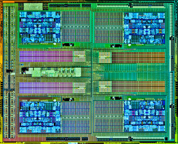
Faced with continuous development roadblocks with TSMC, AMD is reportedly planning to switch to the 28 nm SHP process of GlobalFoundries, to build GPUs in 2015. The 28 nm SHP (super high-performance) node will allow the company to lower voltages, giving it greater room to increase clock speeds of its upcoming GPUs. AMD's GPUs in 2015 could be based on its latest Graphics CoreNext 1.2 architecture, and AMD needs every means to minimize voltages, and crank up clock speeds.

The company hasn't abandoned TSMC completely just yet, with reports speaking of AMD using the Taiwanese fab's 16 nm FinFet node to manufacture its next-generation "Zen" CPUs. Zen is the successor to AMD's "Bulldozer" architecture and its derivatives ("Piledriver" and "Steamroller.") It could feature a radically different core design.
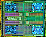
Source: BitsandChips.it
Add your own comment

48 Comments on AMD to Switch to GlobalFoundries' 28 nm SHP Node in 2015

#1
the54thvoid
Intoxicated Moderator
Did AMD benefit from divesting Glo-Fo in 2009? Obviously they received a substantial sum but it's an ongoing productive business. Or does TSMC have a specific remit for smaller nodes that Glo-Fo doesn't?
Posted on Reply
#2
RejZoR
Can't wait for Zen CPU's and next gen AMD GPU's based on new node.
Posted on Reply
#3
Recus
RejZoRCan't wait for Zen CPU's and next gen AMD GPU's based on new node.
Samsung's 28nm? :D
Posted on Reply
#4
GLD
I am behind the lower power idea. I have a AM1 board and cpu inbound for a dual boot Win 7 daily driver/XP nostalgic game rig.

I am not a fan of the Zen naming though. IDK why, just am not a fan.
Posted on Reply
#5
MaKCuMyC
At that moment Intel will sell 14nm chips. AMD suck in twice.
Posted on Reply
#6
Prima.Vera
MaKCuMyCAt that moment Intel will sell 14nm chips. AMD suck in twice.
Source?
Posted on Reply
#8
Debat0r
MaKCuMyCAt that moment Intel will sell 14nm chips. AMD suck in twice.
Good thing that node size is everything when deciding the performance of a CPU.
Posted on Reply
#9
HumanSmoke
Debat0rGood thing that node size is everything when deciding the performance of a CPU.
Well there is something to be said for halving the BGA package size, and cutting the package height to barely more than a millimetre.
Posted on Reply
#11
dj-electric
Notebooks with fully fledged 14nm Broadwell CPUs are starting to pop up. This gen, even the U-series CPUs are quite agressive in performance, Power aside.

The more time that pass, the deeper my concerens about AMD become.
Posted on Reply
#12
HalfAHertz
the54thvoidDid AMD benefit from divesting Glo-Fo in 2009? Obviously they received a substantial sum but it's an ongoing productive business. Or does TSMC have a specific remit for smaller nodes that Glo-Fo doesn't?
They reduced their losses tremendously by giving away their foundries. Just recently IBM "sold" their factories for the same reason. It's questionable if AMD would have existed today if they did not slash the foundries.
Posted on Reply
#13
GhostRyder
RejZoRCan't wait for Zen CPU's and next gen AMD GPU's based on new node.
Neither can I!

More surprised though that they are sticking to 28nm SHP over the original shrink that was predicted. I guess the issues could not be worked out so it looks like all graphics cards will be waiting for the skip to the next shrink which is going to be quite a cut in size if I do say so myself.
Posted on Reply
#14
Jorge
AMD planned to use both 28nm and some 20nm process for GPU in '15.

Zen will be on FinFET most likely at 16/14nm depending on available production in 2016.

As has been discussed here and elsewhere node size does NOT necessarily equal performance potential. As an example GloFo's 28nm SHP allows AMD to significantly lower voltage and power consumption on their graphics cards over TSMC's 28nm process that AMD has used for GPUs.
Posted on Reply
#15
ZoneDymo
You people are looking at this waaay too much from an enthusiast perspective.
The general population (aka 99% of the buyers of these products) wont give 2 shits whether its 14 or 22nm in their laptops.
Posted on Reply
#16
GhostRyder
JorgeAMD planned to use both 28nm and some 20nm process for GPU in '15.

Zen will be on FinFET most likely at 16/14nm depending on available production in 2016.

As has been discussed here and elsewhere node size does NOT necessarily equal performance potential. As an example GloFo's 28nm SHP allows AMD to significantly lower voltage and power consumption on their graphics cards over TSMC's 28nm process that AMD has used for GPUs.
Indeed, node shrink just is a lot of times only part of the many factors in making the chip more efficient/higher performing.
ZoneDymoYou people are looking at this waaay too much from an enthusiast perspective.
The general population (aka 99% of the buyers of these products) wont give 2 shits whether its 14 or 22nm in their laptops.
True but isn't that the fun of it is looking at it from an extreme situation :P
Posted on Reply
#17
repman244
ZoneDymoYou people are looking at this waaay too much from an enthusiast perspective.
The general population (aka 99% of the buyers of these products) wont give 2 shits whether its 14 or 22nm in their laptops.
Last time I checked, people on this forum ARE enthusiasts and are not "general public".
Posted on Reply
#18
alwayssts
GhostRyderNeither can I!

More surprised though that they are sticking to 28nm SHP over the original shrink that was predicted. I guess the issues could not be worked out so it looks like all graphics cards will be waiting for the skip to the next shrink which is going to be quite a cut in size if I do say so myself.
If their next-gen high-end chip is on 28nm (not counting a Hawaii and/or Tonga refresh), I will be thoroughly surprised. Personally, I chalk this up to either being wrong or misinterpretation.

As was said, this was expected to be a split generation complete with hold-overs and replacements across foundries and processes (like how 7970 became 280x, or Tonga on HPM replaced Tahiti using HP). We know another version of Hawaii is coming, and it wouldn't be surprising to see something Tonga-like stick around either. With that said, I can only imagine amd expected more power-savings and/or performance latitude than they got from HPM considering the relative limitations vs HP. GF is probably less-limiting than tsmc HPM...that doesn't necessarily make it better.

From there, it just becomes a question of when is Fiji, and how long between that and (Bermuda?). If the recent past is anything to go by, it could be a bit between each, but I still expect them to release something on a smaller process in 2015 (to compete with GM200). It's important to remember not only is this par for the course (re-using products) but amd has planned to do split-process stacks before. While eventually Cayman was released, for instance, the original plan was for the halo to be on 28nm, with Barts etc on 40nm. Inversely, what became 4770 was supposed to replace 4870 (but 40nm was a mess and we hence got 4890 on 55nm instead). Any of those combinations could occur again.

Things obviously can and do change, and while GF 28nm is a bit more dense (similar to a half-node shrink at the reg 28nm level; SHP may trade some of that size advantage for speed improvements), it has it's own relative issues. I could see voltage going down (if transistors up), but not necessarily clock speeds going up significantly if a similar product, especially at a higher voltage than they currently use. They may gain a die size advantage and more latitude in possible performance, but the power/heat issue will still remain. While recent amd gpus have been limited in clockspeed relative to other chips on the process (I assume because HPM), and GF may better suit a high-logic design, they can't beat physics....just look at their cpus (when approaching a higher-than-ideal clockspeed/voltage). While they could make something more efficiently tuned, to go substantially upwards and onwards I would imagine they need a bigger jump than just switching to 28SHP at GF.
Posted on Reply
#19
ZoneDymo
repman244Last time I checked, people on this forum ARE enthusiasts and are not "general public".
That's not the point, the point is all these people here that talk about "Concerns" about AMD with being potentially behind Intel with this.
There is really nothing to be concerned about, AMD will be fine.
Posted on Reply
#20
RejZoR
Node size is not the only actor, but it helps. Frankly, at the end of the day, I kinda always buy the stuff that offers me the most performance for the least money. My HD7950 is not the most power efficient either, but the performance it keeps on delivering for the time since I've bought it, it's just awesome. So awesome that I'm still hesitating to buy seemingly superior GTX 970.
Posted on Reply
#21
Assimilator
Debat0rGood thing that node size is everything when deciding the performance of a CPU.
Well if we're comparing Intel and AMD current generation CPUs, smaller node size always means better performance, so...
Posted on Reply
#22
HumanSmoke
alwaysstsIf their next-gen high-end chip is on 28nm (not counting a Hawaii and/or Tonga refresh), I will be thoroughly surprised.
I wouldn't. GloFo are too far away with their Samsung-licenced 14nm process, 20nm means TSMC (and encompasses 16nm FinFET since the FEOL uses the same 20nm process as CLN20SOC) since GloFo shitcanned 20nm performance development (now entirely low power IC) . AFAIK, Lisa Su made reference to GPUs using "20nm and finfet" - it neither states that these were mutually exclusive processes (which would point to 16nmFF late in the year), nor that the GPUs would be anything other than the small-die IC's that the process and process cost would be ideally suited for - and the prime reason that 16nmFF+ is now favoured by Nvidia for a general transistion.
alwaysstsThings obviously can and do change, and while GF 28nm is a bit more dense (similar to a half-node shrink at the reg 28nm level; SHP may trade some of that size advantage for speed improvements), it has it's own relative issues.
AMD's Kaveri APUs already use GloFo's 28nm SHP node. No need to guesstimate from GloFo's marketing estimates, the products and their relative density/leakage/power budget per mm etc. are already available for evaluation.
Posted on Reply
#23
repman244
ZoneDymoThat's not the point, the point is all these people here that talk about "Concerns" about AMD with being potentially behind Intel with this.
There is really nothing to be concerned about, AMD will be fine.
AMD IS behind Intel and if they continue with their current trend they won't have to even bother competing with Intel.
They still have some nice products (APU's) but they have lost the high end and server market.
Posted on Reply
#24
Jorge
AssimilatorWell if we're comparing Intel and AMD current generation CPUs, smaller node size always means better performance, so...
Your comparing apples to oranges which is pointless and misleading. Look at the poor performance gains Intel has made in recent node drops even with CPU new designs. They are averaging around 5-7% gains. AMD gets more than that from fine tuning a current node. That's why arguing over node size is ignorant and futile.
Posted on Reply
#25
ZoneDymo
repman244AMD IS behind Intel and if they continue with their current trend they won't have to even bother competing with Intel.
They still have some nice products (APU's) but they have lost the high end and server market.
no they have not, plenty of servers and "the high end" out there use AMD
Posted on Reply
Add your own comment
Apr 24th, 2024 05:52 EDT change timezone

New Forum Posts

Popular Reviews

Controversial News Posts