News Posts matching #2 nm

Return to Keyword Browsing

Rapidus Could Miss 2 nm Mass Production Timeline Amid SRAM Issues

Japanese semiconductor maker Rapidus might miss the planned timeline for its 2 nm node production, as the company is reportedly struggling with its initial attempts at risk production and trial runs. According to a report by the Japan Times, 2 nm volume production at Rapidus facilities will likely be delayed by a few months due to difficulties in 2 nm production, specifically with SRAM. SRAM consists of tiny bitcells that serve as the foundational building blocks for designs operating on one node, and without functional SRAM, it is simply impossible to achieve normal volume production.

There are reportedly other problems, including dust and particle control, which are impacting Rapidus cleanrooms—where the actual silicon is manufactured—to a point where production may be jeopardized altogether. Engineers are working on fixing these problems with the cleanroom and SRAM cells, which should put Rapidus on the right track. Despite these challenges, the company claims that the 2 nm node will arrive on time without any delays, so we are yet to see how these issues will impact their product delivery pipeline.
Samsung's 2 nm Taylor Fab 2 Reportedly Fully Booked, Mostly by AMD

Samsung has reportedly booked the entire planned output of its second fab in Taylor, Texas, and most of it is going to AMD. According to an exclusive from Korea's Maeil Business Newspaper, citing industry sources, Taylor Fab 2 will make HBM base dies for AMD and NVIDIA on a 2 nm process, with AMD's orders making up the bulk of it. Apparently, AMD's volume alone is enough to stretch the fab's capacity. Samsung declined to comment, saying it can't confirm customer-related details.

These aren't AMD's CPUs or GPUs, though. The base die is the logic chip at the bottom of an HBM stack, and Samsung plans to pair the Texas-made dies with DRAM produced in South Korea and ship them as finished HBM. Its current HBM4 and the sampled HBM4E use 4 nm base dies, so 2 nm or smaller seems aimed at later HBM generations. The deal also follows Lisa Su's visit to Samsung in October, where Samsung reportedly wanted foundry orders from AMD in return for the HBM that AMD urgently needs. A March MOU had already made Samsung the primary HBM4 supplier for the Instinct MI455X.

Intel Confirms "Nova Lake" Uses 18A-P Internal Node, More Details at CES

During the Q3 2026 earnings call, Intel CEO Lip-Bu Tan confirmed that the company's upcoming flagship client CPU, codenamed "Nova Lake," will be produced by Intel Foundry using its 18A-P node. Initially, Intel planned to outsource the main compute tile production for "Nova Lake" to TSMC, utilizing its 2 nm N2 node. TSMC was expected to handle about 60-70% of the production, with the remainder produced in-house by Intel Foundry on the 18A node. This meant Intel would dual-source production for its next-generation chip. However, later supply chain information suggested that the company intended to bring the majority of "Nova Lake" compute tile production in-house, with these compute tiles being made on the Intel 18A-P node. Today, we received confirmation directly from the Intel CEO:
Intel CEO Lip-Bu Tan"Nova Lake," our first Intel 18A-P client product, is tracking ahead of schedule, with design wins expected to be twice those of "Panther Lake" at launch. We look forward to sharing more at CES in January.

Samsung Electronics Announces Third Quarter 2026 Results

Samsung Electronics today reported financial results for the third quarter ended Sept. 30, 2026. The Company posted KRW 195.3 trillion in consolidated revenue, another all-time quarterly high, representing a quarter-on-quarter (QoQ) increase of 14%. Operating profit reached KRW 107.4 trillion, making Samsung Electronics the world's first tech company to exceed KRW 100 trillion in quarterly operating profit.

The Device Solutions (DS) Division posted a QoQ sales increase of 15%, with the Memory Business setting an all-time high for quarterly revenue and operating profit, as semiconductor demand is set to remain robust. The Device eXperience (DX) Division posted a QoQ revenue increase of 8% and recorded an operating loss of KRW 0.8 trillion.

GlobalFoundries Returns to Advanced-Node Race With 7 nm-Class FDX Fusion

Back in the now distant 2018, the semiconductor industry had three major players in contract leading-edge node manufacturing: TSMC, Samsung, and GlobalFoundries. At that time, Intel did not accept external clients. However, as node design became increasingly expensive—requiring multi-billion dollar investments—and more complex, with many players encountering yield and manufacturing difficulties, GlobalFoundries announced that it was stopping its 7 nm node development indefinitely. This left only two companies in the leading-edge race, but GlobalFoundries continued to develop unique semiconductor solutions that did not focus on smaller transistor sizes.

Today, the company is back at a similar stopping point but with a unique solution called FDX Fusion, based on fully-depleted silicon-on-insulator (FD-SOI) technology. Unlike traditional CMOS, GlobalFoundries takes substrate isolation a step further by creating a fully insulating layer beneath the channel. This enables highly specialized capabilities, such as ultra-low-power in-memory computing, seamless integration of embedded non-volatile memory (like eMRAM), and highly efficient dense logic designs. With FDX Fusion, GlobalFoundries claims 7 nm-class node characteristics in terms of size and twice the transistor density of the first-generation 22FDX node, which was designated as a 22 nm-class design.

TSMC to Scale 2 nm Production to 120,000 Wafers per Month by the End of 2026

TSMC has reportedly started expanding its manufacturing capacity as demand continues to outpace supply. According to a recent report from UDN, TSMC aims to increase its 2 nm manufacturing capacity at the N2 node, targeting an output of about 120,000 wafers per month by the end of 2026. This represents a 20% increase from the early August target of 100,000 wafers per month by the end of the year, indicating strong customer interest in the latest silicon technology. Even in the early stages, the company confirmed that the N2 node has four times the number of tape-outs compared to its previous leading-edge 3 nm N3 node. With the ramp-up of N2 production underway, the 20% increase suggests that customers are seeking more capacity, even as TSMC continues to scale production, indicating that demand isn't slowing down anytime soon.

At the end of the second quarter of 2026, the N2 node accounted for only 3% of TSMC's revenue, while the 3 nm node held 30%, and the 5 nm node secured the top spot at 33%. However, as we approach the end of Q3, we should see a significant shift in these figures, strongly favoring the N2 node. Until official data is released, we can't be certain of N2's exact revenue contribution, but it is expected to increase significantly based on several factors.

Qualcomm Unveils the Snapdragon 8 Elite Extreme Gen 6 and Snapdragon 8 Elite Gen 6

Qualcomm Technologies, Inc. unveiled today its newest premium mobile lineup - the Snapdragon 8 Elite Extreme Gen 6 Mobile Platform and Snapdragon 8 Elite Gen 6 Mobile Platform. Designed to meet the evolving needs of consumers and OEM partners, both platforms power a new generation of mobile experiences.
Chris Patrick, Senior Vice President and General Manager of Mobile Handsets, Qualcomm Technologies, Inc"Today marks a milestone as we introduce not one, but two new flagship mobile platforms, delivering agentic AI experiences that are immediate, personal, and adaptive," "As the agentic AI age evolves, our multi-flagship strategy allows us to push the boundaries of what's possible for mobile while bringing our latest AI innovations to a broader range of premium devices. By designing two innovative platforms, we're giving OEMs greater choice as we collectively shape the capabilities of the next generation of intelligent, personalized, mobile experiences."

Fujitsu Launches Made-in-Japan Next-Generation CPU Fujitsu-MONAKA and Fujitsu MONAKA Server

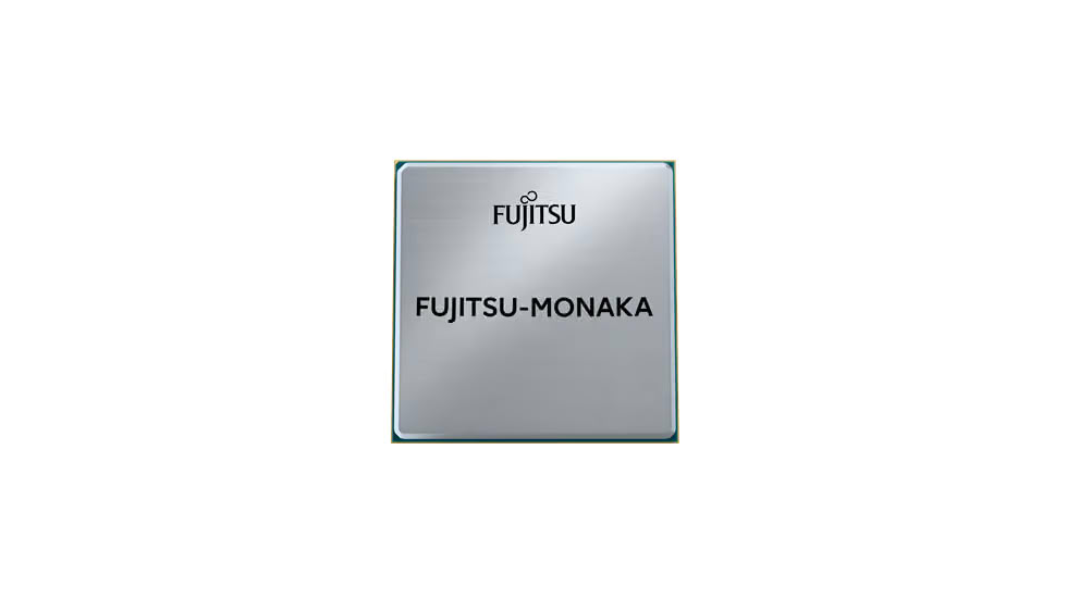
Fujitsu Limited today announced that it will begin global sales of its next-generation CPU, FUJITSU-MONAKA, designed and developed in Japan, starting November 2026. This will include sales of the processor as a standalone product to cloud and data center operators and server vendors. Additionally, the company will launch the made-in-Japan Fujitsu MONAKA Server equipped with the FUJITSU-MONAKA CPU, offering high reliability and power efficiency as a sovereign AI infrastructure. Fujitsu MONAKA Server will be made broadly available from November 2026 to data center operators, enterprises, and the academic and HPC sectors in Japan and Europe, as well as to the defense sector, contributing to national security.

The FUJITSU-MONAKA CPU integrates Fujitsu's extensive expertise in processor and server development, achieving world-class computational performance and data supply capabilities with a maximum operating frequency of 3.8 GHz and memory transfer speed of 8800 MT/s. It delivers twice the AI inference throughput and superior power efficiency compared to other CPUs, effectively halving the number of servers and power consumption required for equivalent processing loads.

TSMC Reports Record $16.26 Billion August Revenue

TSMC today announced its financial results for August, reporting NT$514.81 billion, or about $16.26 billion at the time of writing. This represents a significant 10.1% increase from July's $14.49 billion, indicating that demand remains robust. Growing a multi-billion-dollar manufacturing business at double-digit percentages each month is an impressive achievement and a clear sign that customer orders continue to pour in, with no end in sight for the increasing demand for advanced silicon and packaging. Compared to August 2025, TSMC reported a 53.3% increase in revenue this month, suggesting more customers are committing to new nodes and are willing to absorb any price increases TSMC imposes for its wafers.

Total revenue from January to August reached NT$3,386.87 billion, approximately $107 billion, indicating that the year's results will be extraordinary. Unlike quarterly reports, we don't have detailed information on revenue distribution and customer commitments across different nodes. However, data from the Q2 report showed that the N2 node accounts for only 3% of TSMC's revenue, while the 3 nm node contributes 30%, and the 5 nm node leads with 33%. With the recent launch of Apple's iPhone A20 Pro SoC, the share of 2 nm node orders is expected to increase significantly.

Possible AMD RDNA 5 GPU IP Ships Inside a Samsung SoC on 2 nm Node

Today marks the day we see AMD's next-generation RDNA 5 GPU IP inside working silicon, but not in the form you might expect. Thanks to SemiAnalysis's die annotation of the Exynos 2700 SoC from Samsung, we see AMD's new GPU IP shine in a mobile form with the Xclipse 970 GPU. As earlier leaks reported, AMD and Samsung co-developed the Xclipse 970 GPU using AMD RDNA technology and adapted it for mobile. However, the GPU IP has now been upgraded to the latest RDNA 5, making this SoC technically the first RDNA 5-equipped chip that will be shipping. Built on Samsung Foundry's SF2 node, Samsung has designed this SoC with a unique 10-CPU core configuration and a strong GPU to compete with Qualcomm Snapdragon Elite SoCs.

On the CPU front, Samsung uses Arm's off-the-shelf CPU core IP, which includes C2-Ultra and C2-Pro. This setup features a single C2-Ultra big core running at 4.24 GHz, one C2-Ultra running at 3.36 GHz, four C2-Pro cores running at 3.74 GHz, and four C2-Pro cores running at 2.88 GHz, making a total of 10 CPU cores. On the GPU side, the Xclipse 970 packs eight GPU WGPs, each containing two Compute Units. This results in 16 CUs on the GPU front if everything remains the same with RDNA 5 and no changes to the WGP/CU ratio have been made by AMD since the last-generation RDNA 4.

Samsung New Memory Roadmap: HBM5 Aims for 2x Performance, zHBM for 8x

Samsung presented its updated memory roadmap at SEMICON Taiwan 2026, with HBM5 and the upcoming zHBM architecture being the main focus points while setting ambitious goals and expectations. According to Samsung, HBM5 is targeting twice the performance and 20% higher performance per watt compared to HBM4E, alongside a 20% reduction in thermal resistance. As changes, the base die moves from the 4 nm process used in HBM4 and HBM4E to Samsung's in-house 2 nm node, and the stack options expand to 12, 16, and 20 layers. Mass production is expected around 2028. Recently, Samsung confirmed at the Hot Chips 2026 conference's Advance Program that the company is preparing to ship HBM4E memory with speeds of 16 Gbps per pin. Samsung is currently shipping HBM4 that works at 11.7 Gbps per pin.

zHBM uses a more radical approach, rather than placing memory beside the accelerator as conventional HBM does, zHBM stacks memory directly on top of the processor, shortening the data path and delivering higher bandwidth and efficiency. With zHBM, Samsung is targeting eight times the raw performance and three times the performance per watt of HBM4E, with thermal resistance reduced by 75-90%. At FMS 2026, Samsung unveiled the industry's first concept models of zHBM and is expected to launch this completely different architecture after 2029. Rethinking the HBM architecture appears to be the direction the industry is heading. NVIDIA recently announced its own NVHBM custom memory that moves the memory controller into the HBM base die rather than keeping it on the compute die.

SK hynix Eyes Intel Foundry for HBM4E Base Die Manufacturing

Intel Foundry might win the contract to manufacture base dies for HBM4E memory from SK hynix, according to the South Korean Herald. Reportedly, SK hynix is considering diversifying its base die supplier from solely TSMC to a dual sourcing strategy involving both TSMC and Intel, with Intel Foundry potentially securing a significant portion of the contract. As readers may recall, HBM4E memory allows for the implementation of a base die with custom logic, with DRAM dies stacked on top. Until now, SK hynix has only considered TSMC for this application, but now Intel is also being considered.

For instance, customers could implement custom logic like memory controllers and PHYs directly on the HBM4E base die, significantly reducing the area occupied by these components on the main compute chiplet. SK hynix would send the design to Intel, which would then provide these base dies to SK hynix. The South Korean memory giant would subsequently stack DRAM on top. This approach would free up space on the main compute tile in any AI accelerator for more processing units, reduce latency, and significantly improve performance. However, the question remains as to which Intel node would be used. Up until HBM3E, SK hynix used its own nodes to manufacture base dies. However, as those are 10 nm class nodes, customers are now requiring something more advanced.

AMD Starts "Zen 6" Desktop Enablement in Linux 7.3

AMD's upcoming "Zen 6" desktop processors are moving closer to release as the company begins Linux kernel support in the latest version 7.3. According to Phoronix, AMD has updated the Host System Management Port (HSMP) kernel module, adding protocol version 7, which is used by the Zen 6 Family 1Ah Model 80H processors. Additionally, there are new AMD PMF platform driver features for these processors, likely referring to the "Zen 6" desktop "Olympic Ridge" processors. The AMD PMF driver now also offers device metrics through a new ioctl interface.

With the "Zen 6" generation, AMD is reportedly increasing its CCD core count to up to 12 instances, whereas the previous-generation CCDs maxed out at 8 cores. For versions with two CCDs, the core count starts at 12 cores and continues with 16 and 20-core models, topping off with the flagship 24-core dual CCD SKU. AMD is able to pack more cores per CCD due to the new manufacturing technology, which is TSMC's N2 2 nm node, providing better transistor density compared to the older nodes used in previous generations.

Apple Introduces M6 and M5 Ultra Processors Series

Apple today debuted M6 in the new Mac mini and M5 Ultra in the new Mac Studio, providing an extraordinary leap in performance and AI capabilities. M6, Apple's first state-of-the-art 2-nanometer chip, advances every compute block, delivering gains across every dimension of performance. The chip features a larger 12-core CPU complex with the world's fastest CPU core, a larger 12-core GPU with Neural Accelerators, a Dual 16-core Neural Engine, and up to 170 GB/s of unified memory bandwidth.

M5 Ultra, the ultimate powerhouse for pro and AI workloads, uses next-generation UltraFusion technology to form a quad-die architecture for the first time in an M-series system on a chip (SoC). The chip includes an up-to-36-core CPU and up-to-80-core GPU with a massive 1.2 TB/s of unified memory bandwidth, 50 percent more than M3 Ultra. With their advanced technologies, these SoCs deliver extraordinary compute with industry-leading power efficiency, empowering users to do even more on a desktop.

IBM Unveils Next Generation Dual-Architecture Processor for IBM Z and LinuxONE

At the annual Hot Chips conference, IBM (NYSE: IBM) today is announcing the first dual-architecture mainframe processor, which is being designed to enable enterprises to run operating systems and applications on both the IBM and Arm compute platforms in future IBM Z and LinuxONE systems. This marks the first processor milestone to emerge from the IBM and Arm collaboration established in April 2026, and represents a significant advance in enterprise computing. The new processor is being developed to allow organizations to run Arm-native Linux environments simultaneously with z/OS and Linux on IBM Z, while benefiting from IBM's established security, reliability, and scale.

With more than 22 million developers worldwide, the Arm software ecosystem supports a broad and growing range of applications from cloud to edge, including the cloud-native and AI software increasingly shaping modern infrastructure. This new processor will bring that ecosystem to the IBM platforms known globally for transaction processing and data-intensive operations. Arm workloads will benefit from IBM's enterprise-grade capabilities, including enhanced reliability, hardware-level fault detection and recovery, advanced encryption, secure key management, and AI acceleration.

Intel "Razor Lake" to Use TSMC's N2X Node, Brings bLLC to Laptop SKUs

Intel's "Razor Lake" is a next-generation processor lineup set to launch after the upcoming "Nova Lake" Core Ultra 400 series, scheduled for early 2027. Today, we learn that Intel is planning some "Razor Lake" production to be done on TSMC's N2X node, which is also scheduled for 2027. According to a well-known Intel leaker, Jaykihn, Intel's node of choice for "Razor Lake" will be the enhanced 2 nm design from TSMC. The N2X node is part of the N2 node family but is designed to maintain high frequencies at the cost of some power efficiency compared to the standard N2. This suggests that Intel is preparing to boost frequencies for its next-generation designs, likely to compete with AMD and introduce a performance-leading design.

However, N2X might not be the only node used for production, as Intel is known for dual-sourcing compute tiles, similar to the approach with the upcoming "Nova Lake." Last month, rumors emerged that Intel initially planned to outsource the main compute tile production for "Nova Lake" to TSMC, utilizing its 2 nm N2 node. The majority of the production, about 60-70%, was to be handled by TSMC, with the remainder produced in-house by Intel Foundry on the 18A node. This meant Intel would dual-source production for its next-generation chip. However, the latest supply chain information suggests that the company now intends to bring the majority of "Nova Lake" compute tile production in-house, with about 80-90% of the tiles being manufactured by Intel Foundry. The same could happen with "Razor Lake," depending on the performance of the 18A-P node. Image below is just an illustration.

TSMC Reports Record $14.49 Billion July Revenue

TSMC reported its revenue for July, indicating that the company continues to increase its output capacity, customer commitments, and business execution. TSMC's July revenue stood at NT$467.58 billion, or about $14.49 billion at the time of writing. This marks a 5.6% increase from June's revenue of $13.75 billion and a significant 44.7% year-over-year growth. This suggests that TSMC nearly doubled its July revenue in an environment where it was already selling all its available wafer capacity, indicating rising demand from customers, increasing commitments, and a sustained AI expansion boom.

Revenue for the period from January through July 2026 totaled NT$2,872.06 billion, or about $89.03 billion, representing a remarkable 37.0% increase compared to the same period in 2025. In June, TSMC successfully began high-volume manufacturing of the N2 process. Currently, the N2 node accounts for only 3% of TSMC's revenue, while the 3 nm node contributes 30%, and the 5 nm node leads with 33%. TSMC's fabs currently produce about 20,000 wafers per month on the latest 2 nm N2 node. However, the company is rapidly scaling its high-volume manufacturing, aiming to produce about 100,000 N2 wafers per month by the end of 2026. This scaling up is driving revenue growth. Even with projected increases in N3 and N5 consumption, increasing revenue fivefold would mean the N2 node would represent more than 10% of the company's overall revenue share. Since N2 wafers are naturally more expensive, revenue growth for TSMC has only just begun.

TSMC Targets 100,000 N2 Wafers per Month by the End of 2026

If readers recall, a few days ago we reported that TSMC has achieved a milestone of about 20,000 wafers per month on the company's latest 2 nm N2 node. However, the company is now rapidly scaling its high-volume manufacturing, aiming to produce about 100,000 N2 wafers per month by the end of 2026. This gives the company about four months to increase its manufacturing output fivefold. While that might seem impossible, TSMC has been rapidly scaling its manufacturing output over the years, and the latest N2 node is no exception. Currently, the N2 node accounts for only 3% of TSMC's revenue, while the 3 nm node holds 30%, and the 5 nm node secures the top spot at 33%. Even with projected growth in N3 and N5 consumption, increasing revenue fivefold would mean the N2 node would represent more than 10% of the company's overall revenue share.

Meanwhile, the demand for its 3 nm N3 family of nodes is still strong. Reportedly, TSMC's customers, including NVIDIA, AMD, Broadcom, and many others, have pushed the total monthly wafer output of the N3 node to 180,000 units, exceeding the company's internal targets. While TSMC hoped to achieve this number in the fourth quarter of 2026, demand has pushed production capacity to its limits, prompting TSMC to consider additional expansion plans for this node.

TSMC's 1.4 nm Fab Set for Completion by April 2027

TSMC's 1.4 nm fab for its A14 node is currently under construction, and according to Taiwan's Commercial Times, the project is expected to be completed by April 2027. This is an impressive timeline for TSMC, which began construction of Taichung Phase II in the expansion area of the Central Taiwan Science Park. If everything goes according to plan, this will allow TSMC to scale the A14 node and start trial production late next year, with mass production set to commence in the middle of 2028. These timelines are progressing much faster than TSMC initially expected, and the company can thank modern technology for this acceleration.

Reportedly, TSMC is using artificial intelligence and virtual reality to aid in the fab's development. AI is being used for image recognition and smart inspection, while VR simulations assist with training for high-altitude work and potential hazard situations. This rapid training, construction aid, and everything combined are enabling TSMC to deliver the fab ahead of the company's internal schedules, allowing the A14 node to scale from zero to initial trial production by the end of 2027.

TSMC Hits 20,000 Wafers Per Month Milestone on 2 nm Node

TSMC has reportedly reached a new milestone in scaling its 2 nm node high-volume manufacturing, now producing 20,000 wafers per month on the N2 node alone. Manufactured across five fabs in Taiwan, the company currently has only one fab in volume production on the N2 node. This is reportedly Fab 20, which has reached this figure. TSMC began high-volume production of its N2 node in the fourth quarter of 2025. Fast-forward two quarters to today, and the 2 nm node now accounts for only 3% of the company's revenue, while the 3 nm node commands 30%, and the 5 nm node holds the top spot at 33%.

Recently, the company confirmed that the N2 node has four times the number of tape-outs compared to its previous leading-edge 3 nm N3 node. With GAAFET technology, TSMC's N2 delivers up to a 15% performance increase at the same power level or up to a 30% power reduction at the same speed. This has driven four times the number of customers doing tape-outs, including AMD with its EPYC "Venice" server CPUs, Apple with its A20 Pro chips for the iPhone 18 Pro series, and many others. Even though the N2 ramp now accounts for a small portion of revenue and wafer output, the majority of the business is gradually heading in that direction.

Samsung Electronics and Broadcom Expand Strategic Collaboration Across Memory and Foundry Technologies

Samsung Electronics and Broadcom today announced the signing of a memorandum of understanding (MOU) to expand their strategic collaboration across memory and foundry technologies, supporting the next generation of AI infrastructure. The MOU was announced during the AI Summit, held at The Midway in San Francisco. Attendees included Jinman Han, President and Head of Samsung Electronics' Foundry Business, Hock Tan, President and CEO of Broadcom, senior executives from both companies and representatives of the Korean government. The companies expect the collaboration to be estimated at more than $200 billion across memory and foundry over the next five years through 2030.

On the memory front, Samsung and Broadcom plan to pursue a strategic collaboration for the supply of industry-leading memory solutions, including High Bandwidth Memory (HBM), supporting Broadcom's next-generation AI accelerators. In foundry, the companies' collaboration focuses on Samsung's 2-nanometer (nm) and below process technologies for Broadcom's products, including Wireless Broadband Communications (WBC) solutions. The collaboration is expected to extend to advanced packaging technologies built on Samsung's 2 nm process, including 2.3D and 2.5D integration, to enable higher-performance and more power-efficient AI and networking silicon.

AMD Instinct MI400 Series and Helios Rack Debut: CDNA 5 Goes 2 nm, Plus ROCm.ai and "Gorgon Halo"

AMD used its Advancing AI 2026 keynote today to launch the Instinct MI400 Series, its next-generation data-center GPU family, alongside the Helios rack-scale solution and the CDNA 5 architecture that underpins both. CDNA 5 is AMD's first GPU architecture to reach the 2 nm node, with the flagship Instinct MI455X carrying 320 billion transistors across a multi-chiplet package and 432 GB of HBM4. This is a data-center compute architecture, not a Radeon gaming architecture, though some of the design choices in CDNA 5 point to where AMD's future unified gaming/compute architecture could be headed.

The MI400 Series splits into two parts: the Instinct MI455X for frontier AI and AI-factory deployments, and the Instinct MI430X for sovereign AI and HPC. Together with the Helios rack, 6th Gen EPYC "Venice" CPUs and AMD Pensando networking, they form AMD's open answer to NVIDIA's Vera Rubin NVL72. This post also covers the new ROCm.ai software stack and AMD's "Gorgon Halo" client teaser.

ASML Considers Price Increase for Low-NA EUV, TSMC Unhappy

According to the latest information from the second quarter financial results, ASML is considering raising prices for its Low-NA EUV tools, which is reportedly upsetting its customers. ASML CFO Roger Dassen has noted that the company is looking into price increases for these tools, aligning its pricing strategy with product value. As the company continues to enhance the productivity of its tools, ASML plans to adjust pricing accordingly. The company operates a business unit called Installed Base Management, which focuses on maintaining and improving existing machines. Most of the recent productivity gains have come from ASML's software that operates EUV machines, and the company recently confirmed that:
ASML CFO Roger DassenWhen it comes to Low-NA pricing, of course, you know that we keep on increasing the productivity of the Low-NA tool. Of course, that gives us a pretty strong runway for potential price improvements going forward... Value-based pricing is the concept that we follow within ASML. In the current environment, of course, the value for customers is higher than in other circumstances.

TSMC's 2 nm Node Gains Momentum with Fourfold Increase in Tape-Outs

TSMC's 2 nm node has reportedly attracted significant client attention, as the company's Senior Vice President, Kevin Zhang, confirmed that the N2 node has four times the number of tape-outs compared to its previous leading-edge 3 nm N3 node. This indicates that many of TSMC's customers, who are also long-time partners, have focused their resources on 2 nm chip designs instead of the 3 nm node PDKs. The driving force behind the fourfold increase in chip tape-outs is the impressive power and performance improvements achieved by the company's first gate-all-around FET nanosheet transistor. With GAAFET, TSMC's N2 delivers up to a 15% performance increase at the same power level, or up to a 30% power reduction at the same speed. This means designers can achieve much higher switching performance within the same power budget as the previous N3E, or reduce power consumption by nearly a third while maintaining the same performance target. Additionally, the transistor density increase is about 15%, allowing for smaller dies with the same functionality or larger dies with more performance.

Interestingly, TSMC began high-volume production of its N2 node in Q4 2025. Fast-forward two quarters to today's date, and the 2 nm node now accounts for only 3% of the company's revenue, while the 3 nm node commands 30%, and the 5 nm node holds the top spot at 33%. However, in the coming quarters, the situation is expected to change as TSMC's customers start receiving more 2 nm chips, and the node's revenue generation grows. Among the N2 customers are AMD with its EPYC "Venice" server CPUs, Apple with its A20 Pro chips for the iPhone 18 Pro series, and others. With four times as many customers using the 2 nm node compared to its 3 nm lithography, TSMC's record-breaking quarterly reports are likely to intensify. Each new node generation brings more expensive wafers due to the increasing complexity of developing a new node, so more tape-outs will significantly boost TSMC's revenue. We are yet to see just how substantial the changes will be in the next few quarters.

Samsung Texas Fab to Mass-Produce Tesla AI5 SoC on 2 nm Node

Earlier this year, Elon Musk announced that Tesla had completed the design of its AI5 SoC. Today, we learn that the company will receive these processors from a United States-based Samsung fab located in Taylor, Texas. This means Samsung is preparing to produce the AI5 chip on its SF2 2 nm node on U.S. soil, effectively utilizing the CHIPS Act funding it received to manufacture silicon for domestic companies. As more companies push for domestic manufacturing, Tesla has been working with Samsung and TSMC to leverage their American-based facilities to align the vital parts of the supply chain with the location where the company is based and conducts most of its business.

For Samsung, this is a significant customer win, as Tesla will undertake major volume production in its Taylor fab on the SF2 node. This is one of the first major projects outside of Samsung's usual operations in South Korea, where most of its leading-edge production occurs. Regarding the AI5 chip, Tesla has designed these processors for Full Self-Driving (FSD). The CEO also mentioned that the AI5 chip will offer performance comparable to NVIDIA's "Hopper" architecture, with two AI5 units matching the power of a single "Blackwell" processor. On both the left and right sides, there are two rows of SK hynix LPDDR5X memory modules, each with three modules. This totals 12 LPDDR5X memory modules per AI5 chip. With 16 GB per module, this results in 192 GB of LPDDR5X memory per AI5 SoC. Additionally, Tesla has ambitious plans for nine-month design cycles for the AI6, which will also be part of the joint effort between Samsung, TSMC, and possibly even Intel with its advanced packaging. Musk confirmed that the AI6 and Dojo 3 projects, among other "exciting chips," are currently in progress, suggesting we could see much more custom silicon ASICs in the coming months.
Return to Keyword Browsing
Nov 22nd, 2026 17:40 CST change timezone

New Forum Posts

Popular Reviews

TPU on YouTube

Controversial News Posts