News Posts matching #2 nm

Return to Keyword Browsing

Samsung Ships HBM4 Samples to Customers, Mass Production in 2026

Samsung has just reported its third quarter 2025 results, and the company has confirmed that its next-generation HBM4 memory samples has been shipped to customers worldwide, with mass production expected in 2026. "HBM3E is currently in mass production and being sold to all related customers, while HBM4 samples are simultaneously being shipped to key clients," notes Samsung, confirming that its memory business is thriving and advanced memory solutions are in great demand. In addition, the company has confirmed that "In 2026, the Foundry Business will focus on providing a stable supply of new 2 nm GAA products and the HBM4 base-die, and beginning operations at the Company's fab in Taylor, Texas in a timely manner."

In an HBM stack, consisting of stacked DRAM dies up to a 12-high, connected with TSVs, there is the possibility of embedding an optional base die with customized logic/accelerator circuitry tailored to a specific need. Companies usually opt for off-the-shelf HBM memory for the standardized pricing model implemented across suppliers like Samsung, Micron, and SK Hynix. However, when ordering quantities so large, like NVIDIA and AMD do, they can request special accommodation features. While this may not be necessarily a compute die that brings TeraFLOPS of power, it will likely be a data processing/logic die that helps route data packets more efficiently, cutting latency and improving performance. Especially during inference, where latency is the most important factor, having a "smarter" HBM could yield sizable, double-digit gains in throughput of tokens.

Samsung Electronics Announces Third Quarter 2025 Results

Samsung Electronics today reported financial results for the third quarter ended Sept. 30, 2025. The Company posted KRW 86.1 trillion in consolidated revenue, an increase of 15.4% compared to the previous quarter. Operating profit increased to KRW 12.2 trillion. The Device Solutions (DS) Division reported a 19% increase in sales quarter-on-quarter (QoQ), with the Memory Business setting an all-time high for quarterly sales, driven by strong growth of HBM3E and server SSDs. Meanwhile, the Device eXperience (DX) Division posted a revenue increase of 11% QoQ due to the successful launch of new foldable phones and solid flagship sales.

Looking ahead to Q4, the rapid growth of the AI industry is expected to open up new market opportunities for both the DS and DX Divisions. The DS Division plans to focus on enhancing its performance by increasing sales of high-value-added memory products tailored to AI. The semiconductor market is expected to remain strong, driven by ongoing AI investment momentum. Meanwhile, the DX Division will strengthen its efforts to launch AI products equipped with the most innovative technologies through open collaborations with leading global partners in respective business segments.
TSMC to Bring More Advanced Manufacturing to Arizona Plant Ahead of Schedule

TSMC's strategy to keep advanced manufacturing primarily in Taiwan might be shifting, as indicated by recent comments from CEO C.C. Wei. During the Q3 earnings call, Wei stated, "We are preparing to upgrade our technologies faster... to more advanced process technologies in Arizona, given the strong AI-related demand from our customers." Previously, TSMC has emphasized that its latest nodes would be developed in Taiwan first, with Arizona following. Currently, TSMC produces N4 4 nm technology at its Arizona facilities and had planned to introduce the N3 node in 2028. However, this plan might change in favor of developing more advanced N2 or even A16 nodes in the coming years, as Taiwanese facilities advance to the A16 and A14 nodes first. The U.S. fabs will remain one node generation behind the Taiwanese fabs, rather than several generations as initially planned.

The push to accelerate advanced node deployment is largely driven by demand from U.S. customers. TSMC recently confirmed that its most advanced N2 node will begin volume production by the end of the year, with a rapid increase planned through 2026 in Taiwan. This marks the second 2 nm-class node to reach high-volume manufacturing, following Intel's 18A node. The competition from Intel's 18A and the upcoming 14A ramp may have led TSMC to reconsider its strategy for bringing advanced manufacturing to its U.S. facilities. While TSMC plans to add five more facilities at its Fab 21 site, it is yet to be confirmed which nodes will be developed there. With an accelerated timeline, it seems only a matter of time before we see the first Angstrom-era nodes produced on American soil.

TSMC to Begin N2 Volume Production Before Year-End

TSMC announced today that its next-generation N2 node will enter series production before year's end, with a rapid ramp planned through 2026. This is the second 2 nm-class node to achieve high-volume manufacturing, with Intel's 18A node being the first. Last week, Intel confirmed that its Fab 52 is already pushing out 18A wafers in high-volume manufacturing capacity. The TSMC N2 milestone arrives as the manufacturer posted exceptionally strong Q3 financial results, showing that demand for the most advanced chips is moving faster than the industry can add new capacity. Revenue for Q3 was $33.10 billion, reflecting a 40.8% year-on-year gain and a 10.1% quarter-on-quarter increase.

In the third quarter, TSMC processed an astonishing 4.085 million 300 mm wafers, a rise of approximately 22.4% compared to the same period a year earlier, and reported year-over-year revenue growth of nearly 41%, producing roughly $33.1 billion in sales and more than $15 billion in profit for the quarter. Revenue from advanced process families, including all variants of N3, N5, and N7, now accounts for approximately 74% of total sales. By each node, N3 process shipments accounted for 23% of wafer revenue, N5 for 37% and N7 for 14%. The N5 family showed the largest sales increase, reflecting intense demand for AI accelerators and other high-end devices. It is also worth noting that each node carries a different pricing strategy, with newer nodes being significantly more expensive due to the more advanced and involved manufacturing techniques going into them.

Intel 18A Gets Head Start on TSMC N2 with Fab 52 Ramp

Intel announced this week that its Panther Lake processors have entered volume production at Fab 52 using the company's 18A node, which is touted as the first 2 nm-class process to achieve high-volume manufacturing. This milestone gives Intel a slight timing advantage over rival foundries like TSMC, with its N2 node, and Samsung with its SF2 node. However, being first does not guarantee a lasting lead. Customers, partners, and investors will focus on Intel's ability to maintain parametric yields, control manufacturing costs per unit, and expand 18A beyond limited compute tiles. While Intel has shared improvements in defect density and early functional test results, comprehensive parametric yield metrics that demonstrate consistent achievement of power, performance, and frequency targets remain undisclosed. Initial shipments and early ramp figures will determine whether this production start is symbolic or substantive for Intel's manufacturing revival.

At the transistor level, 18A node introduces two major innovations: RibbonFET gate-all-around transistors and PowerVia backside power delivery. RibbonFET replaces vertical FinFET fins with thin horizontal silicon ribbons wrapped by gate material, enhancing electrostatic control, reducing leakage, and allowing shorter gate lengths. Intel reports approximately 5-10% shorter gate lengths when transitioning from FinFET to RibbonFET on 18A and claims over 20% reduction in per-transistor power. PowerVia relocates the power network to the wafer's backside, freeing up front-side metal for signal routing, shortening power paths, and reducing voltage drop at high switching rates. Together, these changes lower switching energy and provide designers with more flexibility to increase frequencies or reduce power consumption in notebooks and other mobile designs.

AMD Officially Confirms 2 nm Process for Instinct MI450 Accelerator

In an interview with Yahoo Finance right after the surprising OpenAI partnership announcement, AMD CEO Lisa Su confirmed that the next generation of Instinct MI450 graphics accelerators will use 2 nm process technology. "We are very excited about our MI450 generation. It has 2 nm technology, the most advanced fabrication capability," AMD CEO Lisa Su said. AMD uses TSMC's capabilities and technology, having been a loyal partner of the Taiwanese company for years. More details recently leaked from Kepler_L2 show that the TSMC N2P (2 nm) node is only used for the XCD (Accelerator Core Die), while the AID (Active Interposer Die) and MID (Media Interface Die) use the TSMC N3P process.

MI450 is set to go head-to-head with NVIDIA's Rubin generation, which uses the TSMC 3 nm (N3P) process. AMD said MI450 will deliver similar FP4/FP8 performance but with 1.5x more memory and bandwidth. AMD will use the TSMC 2 nm node for both Instinct MI450 and the next-generation EPYC "Venice" server processors, with the accelerators expected to be larger and much more complex to make. As we reported earlier, credible rumors suggest AMD will use Samsung HBM4 memory chips for the Instinct MI450 accelerators—though AMD hasn't confirmed this yet. With the year ending and CES 2026 just three months away, AMD is expected to showcase the next-gen Instinct MI400 series (and possibly even the new EPYC "Venice" generation) in January.

Applied Materials Unveils Next-Gen Chipmaking Products

Applied Materials, Inc. today introduced new semiconductor manufacturing systems that boost the performance of advanced logic and memory chips foundational to AI computing. The new products target three critical areas in the race to deliver ever more powerful AI chips: leading-edge logic including Gate-All-Around (GAA) transistors, high-performance DRAM including high-bandwidth memory (HBM), and advanced packaging to create highly integrated systems-in-a-package that optimize chip performance, power consumption and cost.

"As chips become more complex, Applied is focused on driving materials engineering breakthroughs to provide the performance and power-efficiency improvements needed to scale AI," said Dr. Prabu Raja, President of the Semiconductor Products Group at Applied Materials. "We are collaborating earlier and deeper with our customers to co-develop solutions that accelerate chipmaker roadmaps and enable major device inflections in logic, memory and advanced packaging."

MSI Almost Confirms "Zen 6" Coming to Socket AM5

An MSI representative, without taking names, confirmed that the company's AMD 800-series chipset motherboards will "be ready for future CPUs," in response to a question on whether they support "Zen 6." This would be the first near-confirmation from a motherboard manufacturer that AMD is readying its Ryzen "Olympic Ridge" desktop processor for Socket AM5. This would make "Zen 6" the third microarchitecture for the socket, in line with how AMD released three microarchitectures for its previous Socket AM4.

"Olympic Ridge" will be a chiplet-based processor much like all AMD Ryzen desktop chips going back to the Ryzen 3000 series. These are expected to feature "Zen 6" cores in CPU complex dies (CCDs) built on the 2 nm TSMC N2 process, with AMD expected to increase CPU core counts per CCD for the first time in all these generations. The chip is also expected to introduce a new client I/O die (cIOD) very likely built on the 4 nm TSMC N4P node, which will come with significantly lower TDP than the current one built on 6 nm, and come with a revamped set of DDR5 memory controllers that supports higher speeds. All this said, AMD is rumored to be working on an even newer desktop socket, the new AM6, with a pin count in the range of 2,100 pins. It's likely that "Zen 7" will be designed for this socket.

Alphawave Semi Delivers Cutting-Edge UCIe Chiplet IP on TSMC 3DFabric Platform

Alphawave Semi (LSE: AWE), a global leader in high-speed connectivity and compute silicon for the world's technology infrastructure, has announced the successful tape-out of its cutting edge UCIe 3D IP on the advanced TSMC SoIC (SoIC-X) technology in the 3DFabric platform. This achievement builds on Alphawave Semi's established baseline of leading UCIe IP subsystems and presents a significant evolution in the company's chiplet integration capabilities. By leveraging TSMC's SoIC-X advanced 3D packaging technology, Alphawave Semi continues to push the boundaries of power, performance efficiency and bandwidth for next generation datacenter, AI, and HPC applications.

The IP supports face-to-face (F2F) configurations and provides a 10x improvement in power efficiency over traditional 2.5D die-to-die interfaces. It also delivers up to a 5x increased signal density.

Intel Reportedly Begins 18A Production in Arizona, Panther Lake Reveal Set for Oct. 9

Intel kicked off its first Tech Tour in Arizona with big news about its 18A process node, TrendForce reports citing Commercial Times that says Intel started limited shipments to U.S. customers in Q3, with 18A wafers already in production and initial output of its own CPUs expected in Q4. TweakTown reports that Intel will show off its first in-house 18A processor, Panther Lake, on October 9 during the tour. The Economic Daily News notes that the Panther Lake AI PC chip should ship by year-end, with the 18A rollout backing Intel's next three CPU generations. By starting 18A mass production, Intel became the first among foundry competitors to bring backside power delivery to market, while its Arizona fabs becomes the first in the U.S. to hit 2 nm-class mass production.

Intel's Arizona expansion—Fab 52 and Fab 62—comes from a $32 billion investment launched in 2021. Fab 52 alone should reach 1,000-5,000 wafers per month by year-end, ramp to 15,000 in 2026, and eventually hit 30,000. Industry sources cited by Commercial Times say that, alongside U.S. chip tariff policies, Intel's Arizona fabs are becoming a key option for chipmakers. While 18A still falls behind in transistor density, its backside power delivery cuts routing congestion and boosts frequency performance, drawing interest from global tech giants.

Samsung Cuts 2 nm Node Pricing by 33% in TSMC Competition Push

Samsung has cut its 2 nm wafer prices to $20,000 offering a 33% discount compared to TSMC's expected $30,000 per wafer cost, industry reports say. The company aims to draw customers to its underused advanced manufacturing capacity. The Korean chipmaker faces big pressure to get returns on billions it put into cutting-edge fabrication plants across South Korea and the United States. With production lines running below capacity due to few orders, Samsung has started using bold pricing tactics to compete with Taiwan Semiconductor Manufacturing Company's strong market position. Just recently, the company landed a $16.5 billion deal with Tesla to make next-gen AI chips. People in the industry think this team-up might grow to include more chances maybe even making chips for Elon Musk's xAI project.

TSMC keeps its lead in advanced node manufacturing getting major clients like NVIDIA and AMD for its 2 nm process. The Taiwanese foundry plans to start mass production of 2 nm chips in Q4 2025 even with record-high wafer prices at $30,000 per unit. Samsung has always used lower prices to take on TSMC's control of the market, and it seems to remain on the same strategy with discounts up to 33% cheaper than TSMC's prices for similar 2 nm chip-making services.

TSMC Reportedly Secures 15+ Customers for its "N2" 2 nm Node

TSMC is reportedly handling a significant volume of orders, with 15 or more customers designing on its latest "N2" 2 nm node. According to KLA's Ahmad Khan and Bren Higgins, this N2 node is attracting considerable interest, with 10 of these customers focused on high-performance computing (HPC) designs. Potential clients could include Intel, NVIDIA, AMD, and various startups, while the rest may be developing mobile-optimized designs from companies like Apple, Qualcomm, and MediaTek. "As we're seeing today, the N2 node has about 15 customers working on designs, with around 10 focused on high-performance computing. This is driving rigorous performance requirements," noted KLA's team at a Goldman Sachs conference.

TSMC's N2 node is noted for its high power efficiency and a transistor density of 236.17 million transistors per mm², making it an excellent choice for both HPC/AI and mobile designs. Although TSMC initially planned to implement a backside power delivery network with this node, this feature has been shifted to the A16 node. The N2 will remain a Gate All Around (GAA) FET design to better control transistor gate leakage, moving away from the older FinFET design that has reached its limits with further miniaturization. TSMC has scheduled the commercial launch of the N2 semiconductor node for the second half of 2026, indicating that major technology companies may start adopting this advanced chip technology by early 2027.

MediaTek's First Chipset Using TSMC's 2nm Process Expected in Late 2026

MediaTek today announced that it is among the first companies to partner with TSMC to successfully develop a chip featuring the enhanced N2P process, taping out MediaTek's flagship system-on-chip (SoC) with volume production expected late next year. Marking a new milestone in the strong partnership between MediaTek and TSMC, this long-standing collaboration continues to yield high performance, power-efficient chipsets for customers in flagship mobile, compute, automotive, data center applications and more.

TSMC's 2 nm technology is the first to adopt nanosheet transistor structure, and N2P represents the next evolution in the 2 nm family, set to deliver improved performance and power efficiency. The first chipset utilizing the new TSMC N2P process is expected to be available in late 2026.

Rapidus 2HP 2 nm Node to Match TSMC N2 on Logic Density

According to Korean analyst Kurnal on X, Rapidus, the Japanese foundry pushing into leading-edge chips, will deliver its upcoming 2 nm process, called 2HP, with a transistor density that rivals the best in the business, even TSMC. The reporting allegedly shows a logic density of 237.31 million transistors per square millimeter for 2HP, essentially matching TSMC's N2, which has 236.17 MTr/mm², and comfortably ahead of Intel's 18A at about 184.21 MTr/mm². Rapidus has focused on high-density standard cells and a single-wafer front-end method that allows engineers to tune runs before scaling. It states that a 2 nm gate-all-around test chip built with ASML EUV tools met its electrical targets. The firm plans to publish process design kits in early 2026 and aims to start high-volume production at its IIM-1 facility in 2027, with monthly output expected to reach roughly 25,000 wafers.

What Rapidus is selling beyond raw density is speed and flexibility. While being a node or two behind TSMC in 2027, the company promises significantly shorter cycle times than traditional batch processes, reducing the typical turnaround from around 120 days to approximately 50 days, and offering extreme "hot lot" pushes down to 15 days for urgent orders. To deliver this, Rapidus is building a custom backend ecosystem with OSATs, EDA vendors, IP providers, and materials partners, and it benefits from government support and interest from major compute players. However, density is only one metric of the new node. Energy efficiency, performance per watt, mature supply chains, and, crucially, repeatable yields will determine whether Rapidus can turn validated test silicon into a reliable, high-volume competitor.

Samsung's Second-Gen 2 nm GAA Node Is Make-or-Break for Its Foundry Business

As we have seen with Intel, leading-edge node development is a difficult thing to maintain, unless you are TSMC. It appears that Samsung's push into cutting-edge nodes now hinges on the success of its 2 nm GAA process, which will be a make-or-break node for Samsung Foundry. As the first 2 nm product, Samsung envisioned its own Exynos 2600 flagship SoC for the first-generation SF2 node. However, potential external clients are watching closely to see whether Samsung can translate its development progress into reliable, high-yield manufacturing. This is an area where the 3 nm SF3 node reportedly struggled. If the first 2 nm ramp proves stable, it would validate months of engineering work and reopen opportunities for large-scale foundry contracts. Adding to the pressure, Samsung is already preparing a second-generation variant, known as SF2P, and work on an SF2P+ follow-up is underway. These next steps are important because they promise further gains in performance, power efficiency, and density.

Reports of a major multi-billion Dollar agreement to supply AI-focused chips on Samsung's 2 nm platform have increased expectations and put faith in Samsung's Foundry capability. Such a contract would be a meaningful commercial win, but it will count for little unless Samsung can deliver steady yields and predictable capacity. In the long term, Samsung expects multi-year demand for 2 nm wafers, which is why it is developing multiple process generations in parallel. Nevertheless, the company's reputation in bleeding-edge foundry work will be decided by whether SF2 variants, especially second-generation SF2P and SF2P+, mature quickly enough to offer both the technical benefits and manufacturing reliability customers require. Proving the first 2 nm node can scale is crucial. Still, Samsung's future competitiveness will ultimately rest on stabilizing yields and showing that its second-generation processes can sustain performance and supply over time.

AMD Prepares EPYC "Venice" Platform to Break the 1,000 W Power Barrier

The kilowatt era of CPUs is upon us, as AMD is preparing specialized cooling for its next-generation SP7 socket powering EPYC "Venice". During the OCP APAC 2025 Summit in early August, Microloops held a presentation dedicated entirely to system-level cooling using custom high-performance cold plates, cooling distribution units, and much more. However, an interesting tidbit is the mention of AMD and its plan to likely cool CPUs with TDPs ranging from 700 to 1400 W. This marks AMD's first step into a kilowatt-level chip design, requiring kilowatt-level cooling. AMD is preparing to roll out its Zen 6 microarchitecture in 2026, with a server-focused flagship called EPYC "Venice." The new platform is expected to significantly increase core counts, utilizing full-sized Zen 6 cores and an updated I/O subsystem to target much stronger multithreaded throughput. AMD is reportedly configuring Venice to support as many as 256 CPU cores in a single package, a big leap intended to sharpen its position in dense compute environments.

Under the hood, Zen 6 CCDs are planned for TSMC's 2 nm N2 node, while the server I/O die will bring next-generation connectivity with PCIe Gen 6, doubling raw device bandwidth for GPUs, NVMe storage, and high-speed NICs. AMD has also pointed to memory bandwidth claims of up to roughly 1.6 TB/s, which could be achieved through faster DRAM clocks, expanding the memory controller to a 16-channel DDR5 layout from the current 12 channels, or supporting multichannel DIMM formats such as MR-DIMM and MCR-DIMM. Taken together, AMD says Venice will deliver approximately a 70% improvement in multithreaded performance compared to the current EPYC "Turin" family. However, all of that is shaping up to come with a significant power cost, as AMD gears up to cool these chips through customized solutions.

Marvell Unveils Industry's First 64 Gbps/wire Bi-Directional Die-to-Die Interface IP in 2nm to Power Next Generation XPUs

Marvell Technology, Inc. (NASDAQ: MRVL), a leader in data infrastructure semiconductor solutions, today announced the industry's first 2 nm 64 Gbps bi-directional die-to-die (D2D) interconnect, enabling chip designers to significantly boost the bandwidth and performance of next-generation XPUs while reducing power and silicon area. Delivering 32 Gbps of simultaneous two-way connectivity over a single wire, the interface IP—also available in 3 nm—sets a new standard for performance, power efficiency, and resiliency to meet the scaling demands of next-generation data centers.

The Marvell 64 Gbps bi-directional D2D interface offers bandwidth density over 30 Tbps/mm, more than three times the bandwidth density of UCIe at equivalent speeds, and a minimal depth configuration that reduces compute die area requirements to 15% compared to conventional implementations. The interface IP is also the industry's first in its class to feature advanced adaptive power management that automatically adjusts device activity to bursty data center traffic. This innovation reduces interface power consumption by up to 75% with normal workloads and up to 42% during peak traffic periods.

TSMC Will Have Four 2 nm Plants by 2026, Producing 60,000 Wafers Per Month

TSMC is moving quickly toward a major production milestone, aiming to bring four 2 nm fabs online by 2026, with a combined capacity of more than 60,000 wafers per month. In Kaohsiung's Nanzi park, TSMC has already started installing next-generation lithography scanners in Fab 22's new cleanroom. Its existing P1 line is running at roughly 10,000 wafers per month, and teams worked through the night to equip the neighboring P2 hall. Trial wafers from P2 are expected before Christmas, which would increase Kaohsiung's total output to more than 30,000 wafers per month by the end of the year. Meanwhile, a third building, P3, is rising nearby to support the upcoming A16 node, and P4 and P5 are in the early stages of permitting. About 200 km to the north in Hsinchu's Baoshan district, Fab 20 has also made rapid progress. Its P1 section has completed risk-ramp testing and is shifting to full volume production, while P2 is fully tooled and awaiting qualification lots.

Together, they are projected to add another 30,000 to 35,000 wafers this year, and P3 and P4 structures are already under concrete to serve the A14 generation. All four sites will utilize TSMC's first-generation nanosheet architecture, which reduces switching power by 25% and increases transistor density by 15% compared to the 3 nm node. Although each 300 mm wafer will cost approximately US $30,000, a roughly 50 percent premium over current 3 nm wafers, TSMC has already secured more design wins from Apple, Qualcomm, and MediaTek at this stage than it saw for its 3 nm and 5 nm nodes. Analysts estimate that these four fabs could support up to US $2.5 trillion in downstream electronics revenue over the next five years. Construction crews now work around the clock, and the push to reach 60,000 wafers per month is well underway.

AMD Chips Made at TSMC USA to Cost 5-20 Percent More, But Worth it: CEO Lisa Su

In an interview with Bloomberg, AMD CEO Dr Lisa Su revealed that the company's chips manufactured at the U.S. based fab of TSMC will cost anywhere between 5% to 20% more than the ones TSMC makes back home in Taiwan, but assured that the added cost and supply-chain resilience would make the price-hike worth the effort. Su alluded to the lack of supply-chain resilience being sorely felt by the tech industry during the COVID-19 pandemic years, causing significant second order effects across the world economy.

TSMC has a manufacturing facility in Arizona, but its most advanced node is 4 nm EUV, referred to internally as the N4 family of foundry nodes by TSMC. AMD makes various CPUs, GPUs, FPGAs, and other devices on the TSMC N4P node, but the company is transitioning to the new TSMC N2 (2 nm Nanosheet) node, starting with its next-generation "Zen 6" CPU family. It is widely expected that while the CCDs of "Zen 6" based Ryzen desktop and EPYC server processors are based on N2, the company will introduce new-generation I/O dies for both its client and server processors that will be built on TSMC N4P, advancing from the current TSMC N6.

Rapidus Achieves Significant Milestone with Prototyping of Leading-Edge 2nm GAA Transistors

Rapidus Corporation, a manufacturer of advanced logic semiconductors, today announced that prototyping has started for its 2 nm gate-all-around (GAA) transistor structure at Rapidus Innovative Integration for Manufacturing (IIM-1) foundry. The prototype wafers also started to obtain their electrical characteristics. Rapidus new IIM-1 foundry represents a significant advancement over the traditional foundry model. The company is re-imagining how semiconductor factories should think, learn, adapt and optimize processes in real time through cutting-edge methods and technology including:

Fully single-wafer front-end processing: In a single-wafer process, adjustments can be made to a single wafer, inspected and if successful, applied to all subsequent wafers. Single wafer captures more data, enabling AI models to be trained to improve wafer production and increase yields. Rapidus is one of the first companies that will commercialize fully single-wafer processing, which is central to its Rapid and Unified Manufacturing Service (RUMs).

AMD Sampling Next-Gen Ryzen Desktop "Medusa Ridge," Sees Incremental IPC Upgrade, New cIOD

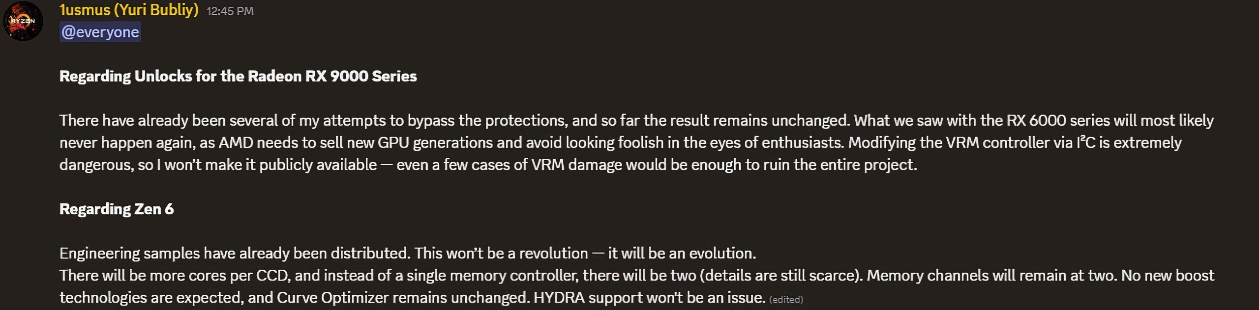
AMD is reportedly sampling its next-generation Ryzen desktop processor powered by the "Zen 6" microarchitecture, codenamed "Medusa Ridge," to close industry partners, such as platform designers and OEMs, says Yuri Bubliy, aka 1usmus, author of the Hydra tuning software, and the now-retired DRAM Calculator for Ryzen. The processor sees AMD update both the CCDs and client I/O die, he says. AMD confirmed that it is building the "Zen 6" CCD on the TSMC N2 (2 nm) node, which entered risk production earlier this year. The node is expected to be ready for mass-production of 2 nm chips later this year. The 2 nm node presents a significant jump in transistor densities from the current TSMC N4P node on which AMD builds its 8-core "Zen 5" CCD, which 1usmus and other sources say, that AMD will use to increase CPU core counts per CCD.

Sources point to the possibility of AMD increasing core counts per CCD to 12, and giving the CCD 48 MB of L3 cache. At this point we don't know if all 12 cores will be arranged in a single CCX with a monolithic slab of 48 MB L3 cache, or if there's a dual-CCX layout with 6 cores per CCX sharing 24 MB of L3 cache, each. The other big upgrade with "Medusa Ridge" is its client I/O die (cIOD). AMD is expected to build its new generation cIOD on a newer EUV node such as 5 nm N5 or 4 nm N4P, a significant upgrade from the current 6 nm N6. 1usmus says that the biggest reason for AMD to update its cIOD is the memory controller architecture. AMD is expected to give "Medusa Point" a new dual memory controller architecture. There are still two DDR5 channels per socket, but this is redesigned for increased memory speeds, letting AMD catch up with Intel in this area. As for the CPU frequency boosting technologies, such as PBO and Curve Optimizer, there are no updates expected, and 1usmus concludes that it Hydra support should be straightforward.

Rapidus Announces Collaboration with Siemens for 2 nm Semiconductor Design

Rapidus Corporation, a manufacturer of advanced logic semiconductors, today announced a strategic collaboration with Siemens Digital Industries Software for semiconductor design and manufacturing processes for the 2 nm generation. Rapidus will collaborate with Siemens to jointly develop a process design kit based on the Calibre platform, the industry-standard verification solution that enables highly accurate and efficient physical verification, manufacturing optimization and reliability assessment from semiconductor design through to fabrication, while continuing to further its design and verification ecosystem.

This collaboration supports the manufacturing for design (MFD) concept advocated by Rapidus to achieve high yield and short turnaround time from the early stages of manufacturing. Further, Rapidus and Siemens EDA will build a reference flow that holistically supports design, verification and manufacturing from front-end to back-end. This reference flow provides a smooth development environment for Rapidus' Rapid and Unified Manufacturing Service (RUMS).

Synopsys Accelerates AI and Multi-Die Design Innovation on Advanced Samsung Foundry Processes

Synopsys, Inc. announced today its ongoing close collaboration with Samsung Foundry to power the next generation of designs for advanced edge AI, HPC, and AI applications. The collaboration between the companies is helping mutual customers achieve successful tape-outs of their complex designs using Synopsys' 3DIC Compiler and Samsung's advanced packaging technologies with fast turnaround time. Mutual customers can improve power, performance and area (PPA) with certified EDA flows for SF2P process, and minimize IP integration risk with the high-quality portfolio of IP on Samsung's most advanced process technologies.

"The adoption of Edge AI applications is driving the need for advancements in semiconductor technologies to enable complex computational tasks, improve efficiency, and expand AI capabilities across various industries and applications," said John Koeter, senior vice president for the Synopsys IP Group. "Together with Samsung Foundry, we're enabling the most advanced AI processors across a broad spectrum of use cases from high-performance AI inference engines for data centers to ultra-efficient Edge AI devices like cameras and drones, all optimized for development on sub-2 nm Samsung Foundry process technologies."

Cadence Accelerates SoC, 3D-IC and Chiplet Design for AI Data Centers, Automotive and Connectivity in Collaboration with Samsung Foundry

Cadence today announced an expansion of its collaboration with Samsung Foundry, including a new multi-year IP agreement to broaden Cadence memory and interface IP solutions in Samsung Foundry's SF4X, SF5A and SF2P advanced process nodes. Furthering their ongoing technology collaboration, the companies are leveraging Cadence's AI-driven design solutions and Samsung's advanced SF4X, SF4U and SF2P process nodes to deliver high-performance, low-power solutions for AI data center, automotive—including advanced driver-assistance systems (ADAS)—and next-generation RF connectivity applications.

Cadence's AI-driven design solutions and comprehensive portfolio of IP and silicon solutions enhance designers' productivity and accelerate time to market (TTM) for leading-edge SoCs, chiplets and 3D-ICs on advanced Samsung Foundry processes. "We support a full portfolio of IP, subsystems and chiplets on the Samsung Foundry process nodes, and our latest multi-year IP agreement strengthens our ongoing collaboration," said Boyd Phelps, senior vice president and general manager of the Silicon Solutions Group at Cadence. "By combining Cadence's AI-driven design and silicon solutions with Samsung's advanced processes, we're delivering the leading-edge technologies our mutual customers need to innovate and bring their products to market faster."

Potential Next-gen AMD EPYC "Venice" CPU Identifier Turns Up in Linux Kernel Update

InstLatX64 has spent a significant chunk of time investigating AMD web presences; last month they unearthed various upcoming "Zen 5" processor families. This morning, a couple of mysterious CPU identifiers—"B50F00, B90F00, BA0F00, and BC0F00"—were highlighted in a social media post. According to screen-captured information, Team Red's Linux team seems to be patching in support for "Zen 6" technologies—InstLatX64 believes that the "B50F00" ID and internal "Weisshorn" codename indicate a successor to AMD's current-gen EPYC "Turin" server-grade processor series (known internally as "Breithorn"). Earlier in the month, a set of AIDA64 Beta update release notes mentioned preliminary support for "next-gen AMD desktop, server and mobile processors."

In a mid-April (2025) announcement, Dr. Lisa Su and colleagues revealed that their: "next-generation AMD EPYC processor, codenamed 'Venice,' is the first HPC product in the industry to be taped out and brought up on the TSMC advanced 2 nm (N2) process technology." According to an official "data center CPU" roadmap, "Venice" is on track to launch in 2026. Last month, details of "Venice's" supposed mixed configuration of "Zen 6" and "Zen 6C" cores—plus other technical tidbits—were disclosed via a leak. InstLatX64 and other watchdogs reckon that some of the latest identifiers refer to forthcoming "Venice-Dense" designs and unannounced Instinct accelerators.
Return to Keyword Browsing
Nov 22nd, 2026 17:51 CST change timezone

New Forum Posts

Popular Reviews

TPU on YouTube

Controversial News Posts