News Posts matching #2 nm

Return to Keyword Browsing

Alphawave Semi Tapes Out New UCIe IP on TSMC 2nm Supporting 36G Die-to-Die Data Rates

Alphawave Semi, a global leader in high-speed connectivity and compute silicon for the world's technology infrastructure, announced the successful tape out of one of the industry's first UCIe IP subsystem on TSMC's N2 process, supporting 36G die-to-die data rates. The solution is fully integrated with TSMC's Chip-on-Wafer-on-Substrate (CoWoS ) advanced packaging technology, unlocking breakthrough bandwidth density and scalability for next-generation chiplet architectures.

This milestone builds on the recent release of the Alphawave Semi AI Platform, proving readiness to support the future of disaggregated SoCs and scale-up infrastructure for hyperscale AI and HPC workloads. With this tape-out, Alphawave Semi becomes one of the industry's first to enable UCIe connectivity on 2 nm nanosheet technology, marking a major step forward for the open chiplet ecosystem.

TSMC Reportedly Surpasses 90% Production Yield Rate with 2 nm Process

At the tail end of Q1'25, industry whispers suggested that TSMC's premier facilities had completed cutting/leading-edge 2 nm (N2) trial production runs. By early April, company insiders alluded to a confident push into preparations for a futuristic 1.4 nm node at the "P2" Baoshan Plant. This is a very distant prospect; watchdogs envision a 2028 release window. According to expert predictions, cross-facility 2 nm wafer mass production phases are expected to start by the end of this year. Foundry staff seem to be actively pursuing an improvement in yields; earlier guesstimates indicated the crossing of a 70% milestone—good enough for full-blown manufacturing runs.

Fresher musings point to staffers and advanced equipment achieving and stepping just beyond an impressive 90% mark, albeit with silicon intended for "memory products." As of mid-May, Samsung's competing "SF2" product—allegedly—remains in testing phases. South Korean insider news reports posit 2 nm GAA trial yields passing 40%—a significant development for the megacorp's foundry business. Roughly a month ago, (in public) TSMC leadership spoke about an unprecedented demand for 2 nm wafers. Due to rumors of greater than anticipated charges for important TSMC clients, Samsung Semi's top brass is supposedly trying to woo the likes of NVIDIA and Qualcomm.

Intel "Nova Lake-S" CPU to Combine Xe3 and Xe4 IPs for Graphics and Media

Intel's "Nova Lake-S" desktop processors are getting the finishing touches, with a likely arrival scheduled for the second half of 2026. As the successor to "Arrow Lake Refresh," Nova Lake-S introduces a modular design that separates graphics and media functions across distinct tiles. This approach builds on experience from "Meteor Lake," which splits its graphics engine from its media and display units onto separate chiplets. For Nova Lake-S, Intel plans to employ two different GPU architectures: Xe3 "Celestial" for graphics rendering and Xe4 "Druid" for media and display duties, all within a single package. Celestial will manage primary 3D rendering and gaming workloads, while Druid will handle display pipelines and hardware-accelerated video encoding and decoding. By utilizing a more advanced process node, such as TSMC's 2 nm, Intel can optimize media engine performance without increasing costs for the entire GPU subsystem.

On the CPU side, Nova Lake-S is expected to span four primary SKU tiers. The flagship model could feature 52 cores (16 P-cores, 32 E-cores, and four LPE-cores). A 28-core version may target high-end laptops and desktops with eight P-cores, 16 E-cores, and four low-power E-cores. A 16-core variant could serve both the lower-power desktop and laptop segments, featuring four P-cores, eight E-cores, and four low-power E-cores. Finally, an 8-core entry-level part offers four P-cores and four low-power E-cores. Although it remains uncertain whether all SKUs will combine both Xe3 and Xe4 tiles, Intel's tile-based strategy makes it straightforward to mix and match GPU configurations for different market segments. Rumors also suggest that Intel may use its 18A node alongside TSMC's advanced processes for various tile elements. As Panther Lake mobile parts approach the second half of 2025 and Arrow Lake Refresh prepares for its desktop release, Nova Lake-S is the pinnacle of Intel's advanced chip packaging.

TSMC Confirms No Middle East Expansion and Anticipates Higher Wafer Costs

TSMC has declared that it has no immediate plans to build fabrication plants in the Middle East, reinforcing its strategy to focus on regions where customer demand is strong. Last week's rumors that TSMC might establish a gigafab in the United Arab Emirates have been dismissed by company executives as baseless. CEO CC Wei explained that an expansion into the Gulf does not fit with TSMC's model of locating factories near its largest clients. With ongoing investments in the US, Japan, and Germany, the company aims to serve technology leaders and automotive manufacturers more effectively. Wei added that, without a solid local customer base, building in the Middle East would be impractical. At the same time, TSMC indicated it is reviewing wafer pricing. Fluctuations in the Taiwanese dollar and changing global tariffs were cited as factors under consideration.

According to Wei, long-term agreements could include modest price increases, especially for advanced process nodes, where research and development costs and manufacturing challenges are rising. Looking ahead, TSMC confirmed that the upcoming A14 1.4 nm node wafers are expected to be priced around $45,000 each. This would represent a 50 percent increase over the current 2 nm wafers, which cost about $30,000 apiece. Production of the 1.4 nm node is projected to begin around 2028. Only TSMC's top-tier customers are likely to reserve capacity for this cutting-edge node in its early stages. As demand for advanced semiconductors rises, the company's approach to pricing and geographic focus will be key to maintaining its leadership in the global foundry market.

MediaTek CEO Anticipates Q4 2025 Taping-out of First 2 nm Chip Design

As previously promised, Dr. Rick Tsai took to the Computex 2025 stage earlier today. The MediaTek CEO's keynote speech included a teaser for next-gen. Currently, the fabless chip design firm's best offerings are manufactured at TSMC foundries—utilizing 3 nm node processes. According to inside track knowledge, the forthcoming Dimensity 9500 mobile chipset will be based on "N3P." During today's important presentation, Tsai announced his company's next major leap—with "2 nm silicon innovation." According to a presentation slide, a tape-out phase is anticipated by this September. Industry experts reckon that a futuristic flagship—perhaps "Dimensity 9600"—SoC will benefit from this generational jump. Finalized products could arrive around late 2026; with MediaTek reportedly being on TSMC's 2 nm (N2) mass production order books. Officially, MediaTek's shift from 3 nm into 2 nm is expected to improve chip performance—with an estimated 15% uplift—while reducing power consumption (by ~25%).

Samsung Foundry Reportedly Making Significant Progress with 2 nm GAA Evaluation Phase

South Korean semiconductor insiders and analysts believe that Samsung's Foundry business is catching up with a main rival. Earlier this month, TSMC leadership openly discussed an unprecedented demand for 2 nm wafer products. Industry moles believe that the Taiwan's top chipmaker is still ahead of contenders in nearby nations. As a result of an alleged leading and comfortable position, TSMC is reportedly upgrading its state-of-the-art facilities with brand-new equipment—indicating a push into 1.4 nm fields. According to a fresh Chosun Biz news article, Samsung engineers are in the process of narrowing the gap between their 2 nm Gate-All-Around (GAA)—also known as SF2—manufacturing node process and TSMC's equivalent technology.

Last month, leaks suggested SF2 trial yields passing the ~40% mark—in comparison, a ~60% figure was uttered by TSMC insiders. Chosun Biz's sources claim that the South Korean foundry team is close to getting their "2 nm process performance evaluation" into a crucial final stage. Yesterday's report posits that NVIDIA and Qualcomm are in the equation; these VIP clients are purportedly considering SF2 as a "second channel" option. Chosun Biz reckons that Team Green is sizing up Samsung Foundry flagship tech for next-gen commercial and enterprise GPUs. Meanwhile, the San Diego-based smartphone processor specialist could be eyeing up SF2 (for a future AP). The latest inside track info points to 2 nm GAA trial production runs breaking beyond aforementioned (approximate) 40% yield rates. TSMC 2 nm wafer charges are reportedly greater than expected, so big industry players are allegedly investigating "cheaper" non-Taiwanese production avenues.

TSMC Leadership Speaks of "Unprecedented" Demand for 2 nm; Greater Than Previous-gen Nodes

Despite recent whispers of TSMC losing a key 4 nm node process customer, industry analysts reckon that Taiwan's premier foundry business will remain in a comfortable leading position for the foreseeable future. "Optimistic" expert opinion points to "revenue growth for supply chain players," driven by the rapid progress of the firm's 2 nm manufacturing prowess. Naturally, their cutting-edge manufacturing capabilities—supposedly bolstered by GAAFET—are being tracked with keen interest. According to a fairly fresh Ctee Taiwan news piece, the usual big players are reportedly queued up and present within factory order books. The likes of Apple, NVIDIA, AMD, Qualcomm, MediaTek and Broadcom are mentioned. Mid-way through last month, Team Red officially announced a big collaborative milestone: "(our) next-generation AMD EPYC processor—codenamed "Venice"—is the first HPC product in the industry to be taped out and brought up on the TSMC advanced 2 nm (N2) process technology."

Ctee's report cites recent statements by C. C. Wei. Apparently, the TSMC CEO has stressed (on multiple occasions) that there is "unprecedented" demand for his company's 2 nm production pipelines—far exceeding previous levels for 3 nm. In addition, TSMC reps—who are currently touring the States; hosting technology symposiums—have revealed 2 nm (N2) defect density trends. Ctee outlined these intriguing details: "(N2's) defect density (D0) performance is comparable to that of the 5 nm family, and even surpasses the 7 nm and 3 nm processes of the same period, making it one of the most technologically mature advanced nodes." Wei's foundry team seems to be well ahead of main competition; insiders reckon that alleged equipment upgrades signal a push into 1.4 nm territories. Crucially, mass production of 2 nm (N2) wafers is expected to begin later this year—a cross-facility push was uttered by industry moles.

Samsung "Exynos 2500" Variant Tipped as SoC of Choice for "Galaxy Z Flip 7"

Yesterday, Chosun Daily published a news report that alleges a key "Galaxy Z Flip 7-related" decision made by Samsung leadership. According to smartphone industry moles, the oft-leaked/rumored "Exynos 2500" chipset destined to debut in the company's next-gen (horizontal) foldable smartphone design. As stated in the South Korean insider article: "this is the first time that Samsung's own mobile application processor (AP) is being installed in a foldable phone." Prior to 2025, Galaxy Flip Z product lines made use of Qualcomm Snapdragon chipsets. Throughout early 2025, leaks have linked the "troubled" Exynos 2500 mobile processor to futuristic Galaxy Z Flip 7, Fold 7, and affordable "FE" Enterprise Edition models. The emergence of a superior 2 nm "Exynos 2600" flagship chip—apparently tailored for Galaxy S26 devices (2026)—has allegedly relegated the lesser SoC into lower leagues.

Semiconductor industry watchdogs reckon that the "Exynos 2500" will be manufactured via Samsung Foundry's own 3 nm GAA node process (aka SF3). Notebookcheck commented on this odd choice: "industry estimates from earlier suggested (SF3) yields were around 40%, making it less than ideal for mass production. But it seems Samsung decided to proceed anyway to save on costs, and likely give a new lease of life to its struggling foundry business." Jukanlosreve followed up with additional inside knowledge, just after the publication of Chosun Daily's news piece. The keen tracker of foundry-related revelations let slip with this observation: "the Exynos 2500 being used in the Flip 7 is said to be a lower-clocked chip due to its low yield. So it might as well be called the E2500E." Samsung is expected to unveil its Galaxy Z Flip 7 smartphone family during an "Unpacked" July event. Experts believe that Foundry employees will accumulate useful experience from the mass production of 3 nm parts; thus leading to improved output of finalized 2 nm (SF2) production lines.

TSMC Reportedly Begins Construction of Third Arizona Production Location

As disclosed in a new press release—issued by the US Commerce Department—TSMC's North American operation has started another expansion. Last month, Taiwan's leading chip foundry committed a substantial $100 billion investment—eventually leading to a greater production footprint in Phoenix, Arizona. Reports suggest that ground has already been broken, in a low-key manner—as of yesterday (April 29)—at a planned third location, only hours after TSMC's receiving of permits—aka a "thumbs up" from the US government. According to local news outlets, key administrative representatives were in attendance to witness the initiation of construction work. TSMC's third plant is destined to pump out cutting-edge products via a 2 nm (N2) process technology, with Apple, NVIDIA and AMD confirmed as "front of the queue" customers. Despite recent fanfare and celebrations, industry analysts reckon that it will take up to a decade for the foundry's North American operation to solidify a dependable supply chain. In the interim, certain elements will require shipping to overseas locations—for packaging and finalization purposes.

Samsung Electronics Announces First Quarter 2025 Results

Samsung Electronics today reported financial results for the first quarter ended March 31, 2025. The Company posted KRW 79.14 trillion in consolidated revenue, an all-time quarterly high, on the back of strong sales of flagship Galaxy S25 smartphones and high-value-added products. Operating profit increased to KRW 6.7 trillion despite headwinds for the DS Division, which experienced a decrease in quarterly revenue.

The Company has allocated its highest-ever annual R&D expenditure for 2024, and in the first quarter of this year, it has also increased its R&D expenditure by 16% compared to the same period last year, amounting to 9 trillion won. Despite the growing macroeconomic uncertainties due to recent global trade tensions and slowing global economic growth, making it difficult to predict future performance, the Company will continue to make various efforts to secure growth. Additionally, assuming that the uncertainties are diminished, it expects its performance to improve in the second half of the year.

Intel Foundry Gathers Customers and Partners, Outlines Priorities

Today at Intel Foundry Direct Connect, the company will share progress on multiple generations of its core process and advanced packaging technologies. The company will also announce new ecosystem programs and partnerships, and welcome industry leaders to discuss how a systems foundry approach enables collaboration with partners and unlocks innovation for customers.

Intel CEO Lip-Bu Tan will open the event by discussing Intel Foundry's progress and priorities as the company drives the next phase of its foundry strategy. Naga Chandrasekaran, Intel Foundry chief technology and operations officer, and Kevin O'Buckley, general manager of Foundry Services, will also deliver keynotes during the morning session, sharing process and advanced packaging news while highlighting Intel Foundry's globally diverse manufacturing and supply chain.

Snapdragon 8 Elite Gen 2 "for Galaxy" SoC Variant Linked to Samsung 2 nm GAA Node Process

Industry watchdogs have held the belief that Samsung's foundry business has lost several key clients due to alleged yield problems—the South Korean megacorp appears to be diligently working on major improvements with currently "in-progress" manufacturing processes; namely 2 nm GAA (aka SF2). Semiconductor industry insiders believe that TSMC is still leading the way with a recently completed trial run of their own 2 nm design, but rumors of elevated prices have reportedly upset certain important customers. According to a fresh Sedaily news article, Qualcomm has conducted negotiations with Samsung Foundry top brass—semiconductor industry moles claim that a "Snapdragon 8 Elite 2nd generation product" was the main topic of discussion. This next-gen flagship mobile chipset was previously linked to a 3 nm TSMC node, but newer rumors point to a possible spin-off that will utilize a "more advanced 2 nm process"—courtesy of Samsung Electronic's prime "Hwaseong S3" facility.

Sedaily and Jukanlosreve reckon that mass production will kick off at this cutting-edge early next year. Earlier today, Jukanlosreve added extra conjecture/context via a long social media bulletin: "the completed chips are expected to be integrated into Samsung Galaxy smartphones slated for launch in H2 2026. Design work is to finish in Q2 2025, after which mass-production preparations will begin and wafer runs will start in Q1 2026. Output is estimated at roughly 1,000 twelve-inch wafers per month. Given that Samsung's current 2 nm capacity is about 7,000 wafers/month, this project would utilize only around 15 % of its available capacity—suggesting this is a modest order rather than a large-scale win." These predictions have surprised many industry observers; Samsung leadership has seemingly tried to prioritize the in-house Exynos mobile processor designs within futuristic flagship Galaxy smartphone devices. Jukanlosreve reckons that the Samsung Foundry is keen to embrace any new "golden opportunities," given the operation's weakened track record across the past half decade. One unnamed insider posited: "this Qualcomm partnership could pave the way for orders from other big tech players." Sedaily sent a query to Samsung HQ, regarding the latest inside talk—a company spokesperson replied with: "we cannot confirm anything related to customer orders."

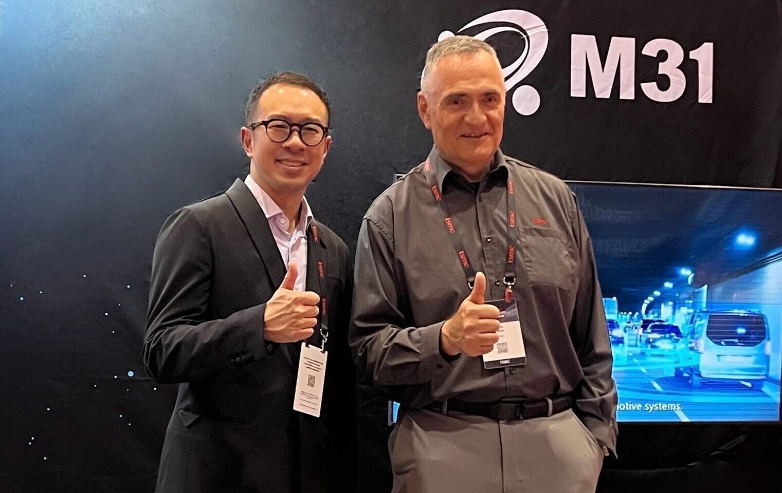
M31 Collaborates with TSMC to Advance 2nm eUSB2 IP Innovation

M31 Technology Corporation (M31), a global provider of silicon intellectual property (IP), today announced that its eUSB2 PHY IP has achieved silicon-proven status on TSMC's 3 nm process and has successfully completed tape-out on TSMC's 2 nm process. As a member of TSMC Open Innovation Platform (OIP) IP Alliance since 2012, M31 has been honored with TSMC OIP Partner of the Year Award for seven consecutive years. In 2020, M31 pioneered its eUSB2 IP solution on the TSMC 7 nm process node, further solidifying its leadership in advanced interface IP development. Since then, M31 has steadily expanded its eUSB2 IP portfolio across TSMC's 5 nm, 3 nm, and most recently, 2 nm process technologies—closely aligning with TSMC's cutting-edge roadmap to accelerate the adoption of AI-enabled smart devices. Looking ahead, M31 is actively developing the next-generation eUSB2 Version 2.0 (eUSB2V2) PHY IP, with ongoing efforts focused on both TSMC's 3 nm and 2 nm process nodes.

Reinforcing its robustness and reliability on advanced nodes, M31's eUSB2 IP solutions have been widely adopted by leading global companies in high-end smartphone chipsets and AI-driven image processing applications. Building on this success, M31 is currently advancing the development of eUSB2V2 IP on TSMC's N3 and N2 process technologies - expanding its comprehensive eUSB2 portfolio to include eUSB2 V1, V2 PHY, and eUSB2 Repeater solutions. Leveraging the eUSB2 standard, eUSB2V2 enhances data transfer rates while maintaining a low-voltage interface and leveraging asymmetric bandwidth technology—allowing TX and RX to operate at different data rates. This significantly improves transmission efficiency, making it ideal for embedded applications such as AI edge computing, smart surveillance, and image processing chips. To accommodate diverse design needs, eUSB2V2 leverages and enhances the I/O architecture based on the eUSB2 standard, supporting data transfer speeds from 480 Mbps up to 4.8 Gbps. The solution delivers a comprehensive eUSB2 platform for high-end SoCs—optimizing power efficiency, performance and design flexibility, while maintaining full compatibility with legacy USB 2.0 devices.

Intel's "Nova Lake" Processors Reportedly Slated for TSMC's 2nm Node

TSMC is pushing forward its plans to make 2 nm process chips in large quantities in the second half of the year, with major customer developments coming to light. After AMD placed its order, reports suggest Intel has also become one of TSMC's first 2 nm customers aiming to use this cutting-edge technology for its next-gen desktop processors. Intel, already a big TSMC customer for advanced processes sent out key compute tiles for its Core Ultra processors to TSMC using different processes like N3B, N5P, and N6. To be exact, these were Intel Core Ultra 200V "Lunar Lake" series laptop processors and Core Ultra 200S "Arrow Lake" series. While both companies didn't comment on the latest news, industry talk hints that they're cooperating on Intel's upcoming Nova Lake desktop processor set to launch next year (rumors suggest that it could be the Compute Tile). With the codename "NVL-S" Nova Lake combines two groups of eight high-performance "Coyote Cove" P-cores with 16 "Arctic Wolf" E-cores. It also includes four ultra-low-power LPE cores in a separate SoC tile. It is expected that Nova Lake-S will use LGA 1954, which has 1,954 active lands and might have more than 2,000 total pads when you count debug pins.

TSMC's work on 2 nm technology is moving forward as expected. The company uses first-generation nanochip transistor technology to boost performance and reduce power consumption across process nodes with big clients finishing designing silicon IPs and starting validation steps. AMD shared that its next EPYC "Venice" chip will be the first high-performance computing processor to use TSMC's 2 nm process. AMD validated it at TSMC's Arizona plant and is on track to launch it in 2026. Also, word has it that Apple's future iPhone 18 lineup will have its A20 chip made with the same TSMC 2 nm process.

AMD Achieves First TSMC N2 Product Silicon Milestone

AMD today announced its next-generation AMD EPYC processor, codenamed "Venice," is the first HPC product in the industry to be taped out and brought up on the TSMC advanced 2 nm (N2) process technology. This highlights the strength of AMD and TSMC semiconductor manufacturing partnership to co-optimize new design architectures with leading-edge process technology. It also marks a major step forward in the execution of the AMD data center CPU roadmap, with "Venice" on track to launch next year. AMD also announced the successful bring up and validation of its 5th Gen AMD EPYC CPU products at TSMC's new fabrication facility in Arizona, underscoring its commitment to U.S. manufacturing.

"TSMC has been a key partner for many years and our deep collaboration with their R&D and manufacturing teams has enabled AMD to consistently deliver leadership products that push the limits of high-performance computing," said Dr. Lisa Su, chair and CEO, AMD. "Being a lead HPC customer for TSMC's N2 process and for TSMC Arizona Fab 21 are great examples of how we are working closely together to drive innovation and deliver the advanced technologies that will power the future of computing."

Samsung's 2 nm GAA Node Process Test Yields Reportedly Pass 40% Mark

According to the latest South Korean semiconductor industry whispers, Samsung's 2 nm GAA node process (aka SF2) development team has hit another pleasing experimental production milestone. An Asia Economy SK news article has sourced insights from inside track players—one unnamed mole posited that: "the 2 nm yield currently under development at Samsung Foundry is much better than previously known...and more positive than the (reportedly abandoned) 3 nm process." A combination of relatively new leadership and a rumored welcoming of first wave High-NA EUV equipment has likely bolstered next-gen efforts, after late 2024's alleged failure of 3 nm prototypes. Leaks from earlier in 2025 indicated SF2 test yields wavering around 20-30%; far from ideal—back then, insider reports suggested that TSMC was well on the way to achieving 60% rates with a competing 2 nm product line. Asia Economy has picked up on mutterings about Samsung's current progress—latest outputs: "have exceeded 40% in the wafer testing stage at a post-processing company."

Industry watchdogs reckon that the South Korean's foundry business is making good progress; perhaps on track to commence speculated mass production by the third quarter of this year—just in time to get finalized flagship "Exynos 2600" mobile chips in the manufacturing pipeline. The Taiwanese rumor mill indicated a major milestone "completion" of TSMC's 2 nm trial phase at some point last month—insiders mentioned excellent yield rates: in the region of 70-80%. Cross-facility mass production could start later this year, but experts propose that the market leader will be implementing price hikes. These "elevated charges" could send loyal TSMC customers in the direction of an alternate source of 2 nm wafers: Samsung. Fresh semicon biz gossip has the likes of Apple, AMD and NVIDIA in the picture.

Leaker Claims that Samsung Will Stop Using "Exynos" Nomenclature, Next-gen 2 nm Mobile SoC Tipped for Rebrand

Over the past weekend Jukanlosreve declared via social media that Samsung's: "Exynos 2600 (mobile SoC) is definitely back, and it will be used in the Galaxy S26 series. But the chip volume is so limited that it'll likely be similar to the Exynos 990 situation. I'm not sure if SF2 is actually any good." Mid-way through March, the keen observer of semiconductor industry conditions posited that Samsung's Foundry business could abandon a 1.4 nm (SF1.4) process node. SF2 (aka 2 nm GAA) seems to be in a healthier place, according to insiders—thanks to rumored assistance from an external AI-specialist partner. The development of next-generation flagship Exynos smartphone processors are allegedly closely tied with Samsung Foundry's 2 nm GAA manufacturing process.

As alluded to by Jukanlosreve's recent prediction, the statuses of leaked 2 nm-based "Exynos 2600" and "Exynos 2500" chips were often questioned by industry watchdogs in the past. The latter is purportedly destined for rollout in forthcoming affordable "Galaxy Z Flip FE" models, albeit in mature 4 nm form. Vhsss_God—another source of inside track info—has weighed in on the topic of Samsung's next-gen chipset roadmap. Compared to Jukanlosreve's musings, their similarly-timed weekend projection seemed to be quite fanciful: "exclusive leak...Samsung doesn't want to use Exynos or Qualcomm Snapdragon chips anymore. S26 line is targeted to launch with the new Samsung developed chip (2 nm)—formerly referred to as Exynos 2600. (The company) will try its hardest to ditch Snapdragon on the entire Galaxy line next year." Perhaps there is too much of a negative stigma attached to Samsung's long-running chipset nomenclature, but the majority of foundry moles continue to label incoming designs as Exynos processors.

Rapidus Confirms Launching 2nm Pilot Line in April, Mass Production Set for 2027

Rapidus Corporation today announced that its plans and budget for fiscal year 2025 have been approved by Japan's New Energy and Industrial Technology Development Organization (NEDO). The approval covers two commissioned projects under NEDO's "Post-5G Information and Communication Systems Infrastructure Enhancement R&D Project / Development of Advanced Semiconductor Manufacturing Technology (Commissioned)." These projects are the "Research and Development of 2 nm-Generation Semiconductor Integration Technology and short TAT (turnaround time) Manufacturing Technology Based on Japan-U.S. Collaboration" and "Development of Chiplet, Package Design and Manufacturing Technology for 2 nm-Generation Semiconductors."

The first of these projects, focused on front-end processes, was launched in November 2022 as part of Japan's next-generation semiconductor R&D effort. Under this program, Rapidus has continued construction of the Innovative Integration for Manufacturing (IIM) facility in Chitose, Hokkaido, which will serve as its production base. It also sent engineers to IBM in the U.S. to jointly develop 2 nm logic semiconductor mass production technologies and continued to achieve target performance as planned. Furthermore, Rapidus has installed EUV lithography and other production equipment at the IIM facility, and started cleanroom operation. As a result of these efforts, the company achieved its performance targets for FY2024.

Report Suggests TSMC's Successful Completion of 2 nm Trial Phase, Cross-facility Mass Production Expected by End of Year

Going back to the start of this year, TSMC's trial run of a cutting-edge 2 nm (N2) node process was reportedly progressing beyond initial expectations. According to industry moles, two flagship fabrication facilities are "optimistically" tipped to pump out 80,000 units per month (by the end of 2025). This cross-facility total figure was linked to TSMC's Baoshan—located near the Northern Taiwanese city of Hsinchu—and Kaohsiung (in the South) plants. The latest regional reports suggest that the aforementioned trial phase was a resounding success, with pleasing results pointing to an "ahead of schedule" transfer to mass production phases. Insiders previously heard about the Kaohsiung production hub's schedule; with mass production set to start by early 2026—according to fresh rumors, revised calendars have a kick-off window repositioned somewhere in late 2025. Apparently a special "2 nm plant expansion ceremony" took place in that location, earlier today.

A noted semiconductor business analyst—Ming-Chi Kuo—reckons that recent 2 nm pilot yields have progressed well over the 60% mark, meaning that the involved foundry teams are more than ready to move onto kicking things into high gear. Taiwan's Economic News Daily anticipates significant financial gains, due to TSMC N2 products already being in high demand: "the quarterly revenue in the second half of the year is expected to reach one trillion yuan (~US$30.1 billion) for the first time, and it is poised to challenge the goal of earning twice the share capital in a quarter and rewrite the record for a single quarter." The local publication claims that TSMC Baoshan's "first batch of production capacity" is fully reserved for Apple, while Kaohsiung will take care of orders for other (i.e. less) important customers.

Rapidus Announces Strategic Partnership with Quest Global to Enable Advanced 2nm Solutions

Rapidus Corporation, a manufacturer of advanced logic semiconductors, today announced that it signed a Memorandum of Cooperation with Quest Global Services PTE. Ltd. As part of the agreement, Rapidus will become Quest Global's new semiconductor foundry partner, enabling it to provide a wide range of solutions to its customers. Quest Global customers will be able to leverage Rapidus' 2 nm gate-all-around (GAA) manufacturing process to develop engineering design and manufacturing solutions that will support growing industry demand for low-power artificial intelligence (AI) semiconductors. Together, the two companies will deliver transformational silicon solutions as a virtual integrated device manufacturer (IDM) model for fabless companies.

The AI semiconductor industry is in its early stages, with applications just beginning to emerge and new entrants quickly coming to market. Customers will shift from general-purpose AI semiconductors to dedicated designs that reduce power consumption and maximize performance. To support these industry requirements, customers will engage design firms focused on providing custom solutions, such as Quest Global, while also collaborating with semiconductor foundries, like Rapidus, that can manufacture dedicated semiconductors with a short turnaround time.

Industry Analyst Walks Back Claim about Apple A20 SoC Using N3P, Repredicts TSMC 2 nm

Earlier in the week, Apple specialist press outlets picked up on a noted industry analyst's technological forecast for a future iPhone processor design. Jeff Pu—of GF Industries, Hong Kong—predicted that the next-generation A20 SoC would be produced via a TSMC 3 nm (N3P) nodes process. Despite rumors of Apple gaining front row seats at the "2 nm ballgame," the partnership between fabless chip designer and foundry could potentially revisit already covered ground. The A19 chipset was previously linked to N3P (by insiders), with Pu expressing the belief that A20 would utilize the same fundamental lithographic underpinnings; albeit enhanced with TSMC's Chip on Wafer on Substrate (CoWoS) packaging technology (for AI improvements).

This morning, MacRumors followed up on their initial news article—they reported that "wires were crossed" at GF Industries, regarding projections for the (2026) iPhone 18 generation. The publication received direct feedback from the man of the hour: "Jeff Pu (lead Apple analyst) has since clarified that he believes the A20 chip will be manufactured with the N2 process, so the information about the chip using the N3P process should be disregarded. Earlier reports had said the A20 chip would be 2 nm, so rumors align again. This is ultimately good news, as it means the A20 chip should have more substantial performance and power efficiency improvements over the A19 chip." Cutting-edge smartphone processor enthusiasts expressed much disappointment when A20 was (regressively) linked to N3P; the latest revisement should instill some joy. According to industry moles, TSMC is making good progress with its cutting-edge 2 nm node process—mass production is expected to start at some point within the second half of 2025.

Apple "A20" SoC Linked to TSMC "N3P" Process, AI Aspect Reportedly Improved with Advanced Packaging Tech

Over a year ago, industry watchdogs posited that Apple was patiently waiting in line at the front of TSMC's 2 Nanometer GAA "VVIP queue." The securing of cutting-edge manufacturing processes seems to be a consistent priority for the Cupertino, California-headquartered fabless chip designer. Current generation Apple chipsets—at best—utilize TSMC 3 nm (N3E) wafers. Up until very recently, many insiders believed that the projected late 2026 launch of A20 SoC-powered iPhone 18 smartphones would signal a transition to the Taiwanese foundry's advanced 2 nm (N2) node process. Officially, TSMC has roadmapped the start of 2 nm mass production around the second half of 2025.

According to Jeff Pu—a Hong Kong-based analyst at GF Securities—the speculated A20 (2026) chipset could stick with N3P. Leaks suggest that aspects of Apple's next in line "A19" and "A19 Pro" mobile SoCs could be produced via a 3 nm TSMC process. MacRumors has picked up on additional inside track whispers; about Apple M5 processors (for next-gen iPad Pro models) being based on N3P—"likely due to increased wafer costs." Pu reckons that Apple's engineering team has provisioned a major generational improvement with A20's AI capabilities, courtesy of TSMC's Chip on Wafer on Substrate (CoWoS) packaging technology. This significant upgrade is touted to tighten integration between the chip's processor, unified memory, and Neural Engine segments. Revised insider forecasts have positioned A21 chip designs as natural candidates for a shift into 2 nm GAA territories.

Samsung Reportedly Partnered Up with Palantir to Improve Chip Production Yields

According to The Korea Economic Daily, an unlikely alliance—involving Samsung Electronics and Palantir Technologies—was formed at the end of last year. Late last week, insiders posited that the South Korean megacorporation's Foundry business was going through troubled times. It is not clear whether the assistance provided by Palantir's AI-infused suite has produced pleasing results chez Samsung's flagship production hubs, but insiders reckon that utilization of the software started just before Christmas. Local media outlets view this unusual pairing as a "gamble"—reportedly, the new-ish initiative has targeted an improved "semiconductor yield (ratio of good products in total production), quality, and productivity."

The Samsung Foundry appears to be going "all-in" with its 2 nm GAA node process; industry moles picked up on signals transmitted by an alleged special "task force (TF)." This elite team is reportedly entrusted with a challenging two-pronged goal; get 2 nm GAA over the finish line by late 2025, alongside the (connected) finalization of a much-rumored "Exynos 2600" mobile chipset. The Korea Economic Daily news article mentions the expansion of a "Samsung DS Division AI Center" back in December (2025), but falls short of labelling this department as the aforementioned "special task force." Despite a previous reluctance to share sensitive data with external companies, the latest report suggests a significant change in strategy. Further details were disclosed: "(Samsung's) collaboration with Palantir is handled by the DS Division AI Center...The AI Center is an organization that merged the DS Division Innovation Center and SAIT (formerly Samsung Advanced Institute of Technology) AI Center, and is developing DS Division-specific technologies using AI, advancing development software, building AI platforms, and controlling and advancing facilities and infrastructure." Around late February, industry inside trackers predicted continued "smooth" progress with the 2 nm GAA node. Samsung Foundry's fully upgraded "S2" mass production line is expected to come online by Q4 2025.

Samsung Reportedly Planning Mass Production of "Exynos 2600" Prototypes in May

Late last month, industry insiders posited that pleasing progress was being made with Samsung's cutting-edge 2 nm Gate-All-Around (GAA) node process. The rumored abandonment of an older 3 nm GAA-based project—in late 2024—has likely sent the South Korean foundry team into overdrive. A speculated Exynos 2500 flagship mobile processor was previously linked to said 3 nm node, but industry watchdogs believe that company engineers are experimenting with a 2 nm GAA manufacturing process. According to the latest insider report—from FN News SK—Samsung Foundry (SF) has assembled a special "task force (TF)." Allegedly, this elite team will be dedicated to getting a newer "Exynos 2600 chip" over the finish line—suggesting an abandonment of the older "2500" design, or a simple renaming.

Samsung's recent launch of Galaxy S25 series smartphones was reportedly viewed as a disappointing compromise—with all models being powered by Qualcomm's "first-of-its-kind customized Snapdragon 8 Elite Mobile Platform," instead of in-house devised chipsets. According to industry moles, one of the SF task force's main goals is a boosting of 2 nm GAA production yields up to "economically viable" levels (roughly 60-70%)—apparently last month's best result was ~30%. Mass production of prototype chipsets is tipped to start by May. Samsung's reported target of "stabilizing their Exynos 2600" SoC design will ensure that "Galaxy S26 series" devices will not become reliant on Qualcomm internals. Additionally, FN News proposes a bigger picture scenario: "the stabilization of 2 nm (SF2/GAA) products, is expected to speed up the acquisition of customers for Samsung Electronics' foundry division, which is thirsty for leading-edge process customers." A forthcoming rival next-gen mobile chip—Snapdragon 8 Elite Gen 2—is supposedly in the pipeline. The smartphone industry inside track reckons that Qualcomm has signed up with TSMC; with a 2 nm manufacturing process in mind.

ASML and imec Sign Strategic Partnership Agreement to Support Semiconductor Research and Sustainable Innovation in Europe

ASML Holding N.V. (ASML) and imec, a leading research and innovation hub in nanoelectronics and digital technologies, today announce that they have signed a new strategic partnership agreement, focusing on research and sustainability. The agreement has a duration of five years and aims to deliver valuable solutions in two areas by bringing together ASML's and imec's respective knowledge and expertise. First, to develop solutions that advance the semiconductor industry and second, to develop initiatives focused on sustainable innovation.

The collaboration incorporates ASML's whole product portfolio, with a focus on developing high-end nodes, using ASML systems including 0.55 NA EUV, 0.33 NA EUV, DUV immersion, YieldStar optical metrology and HMI single- and multi-beam technologies. These tools will be installed in imec's state-of-the-art pilot line and incorporated in the EU- and Flemish-funded NanoIC pilot line, providing the most advanced infrastructure for sub-2 nm R&D to the international semiconductor ecosystem. Focus areas for R&D will also include silicon photonics, memory and advanced packaging, offering full stack innovation for future semiconductor-based AI applications in diverse markets.
Return to Keyword Browsing
Nov 22nd, 2026 17:51 CST change timezone

New Forum Posts

Popular Reviews

TPU on YouTube

Controversial News Posts