News Posts matching #4 nm

Return to Keyword Browsing

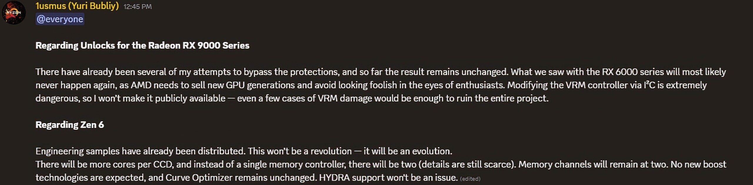
AMD Radeon RX 9070 GRE Tested, Fills Gap Between RX 9060 XT and RX 9070

AMD released the China-exclusive Radeon RX 9070 GRE in May, and ComputerBase.de caught hold of a Sapphire Pulse branded RX 9070 GRE card to test. While the RX 9060 XT specs sheet reads as being exactly half of the RX 9070 XT, the RX 9070 GRE is configured to be three quarters of it. It's based on the same 4 nm "Navi 48" silicon as the rest of the RX 9070 series, but is configured with 48 compute units out of the 64 present, and comes with 12 GB of memory across a 192-bit wide GDDR6 memory bus, in place of the 256-bit wide one that the RX 9070 and RX 9070 XT come with. With 48 CU, the RX 9070 GRE has 3,072 stream processors, 96 AI accelerators, 48 RT accelerators, 192 TMUs, and 96 ROPs. The Infinity Cache size is reduced to 48 MB. The card comes with the same 220 W TBP as the RX 9070.

Testing by ComputerBase.de finds that despite its reduction in compute units and memory, the RX 9070 GRE is still a 1440p-class GPU, and a significant upgrade over the RX 9060 XT 16 GB and the NVIDIA GeForce RTX 5060 Ti 16 GB. Averaged across 13 game tests, at 1440p, the RX 9070 GRE tests 28.4% faster than RX 9060 XT 16 GB, 22% faster than RTX 5060 Ti 16 GB, and 11% faster than the previous-gen RX 7800 XT, and 5% faster than RTX 4070. The current-gen RTX 5070 is 9% faster, RX 9070 is 14% faster, and the current flagship RX 9070 XT is 29% faster. This makes the RX 9070 GRE an interesting SKU that's at the intersection of various price-performance combinations within the 1440p class. In the Chinese domestic market, the RX 9070 GRE is priced slightly higher than the RTX 5060 Ti 16 GB, but lower than the RTX 5070, making it a good value proposition. Find more test results and insights in the source link below.

AMD Sampling Next-Gen Ryzen Desktop "Medusa Ridge," Sees Incremental IPC Upgrade, New cIOD

AMD is reportedly sampling its next-generation Ryzen desktop processor powered by the "Zen 6" microarchitecture, codenamed "Medusa Ridge," to close industry partners, such as platform designers and OEMs, says Yuri Bubliy, aka 1usmus, author of the Hydra tuning software, and the now-retired DRAM Calculator for Ryzen. The processor sees AMD update both the CCDs and client I/O die, he says. AMD confirmed that it is building the "Zen 6" CCD on the TSMC N2 (2 nm) node, which entered risk production earlier this year. The node is expected to be ready for mass-production of 2 nm chips later this year. The 2 nm node presents a significant jump in transistor densities from the current TSMC N4P node on which AMD builds its 8-core "Zen 5" CCD, which 1usmus and other sources say, that AMD will use to increase CPU core counts per CCD.

Sources point to the possibility of AMD increasing core counts per CCD to 12, and giving the CCD 48 MB of L3 cache. At this point we don't know if all 12 cores will be arranged in a single CCX with a monolithic slab of 48 MB L3 cache, or if there's a dual-CCX layout with 6 cores per CCX sharing 24 MB of L3 cache, each. The other big upgrade with "Medusa Ridge" is its client I/O die (cIOD). AMD is expected to build its new generation cIOD on a newer EUV node such as 5 nm N5 or 4 nm N4P, a significant upgrade from the current 6 nm N6. 1usmus says that the biggest reason for AMD to update its cIOD is the memory controller architecture. AMD is expected to give "Medusa Point" a new dual memory controller architecture. There are still two DDR5 channels per socket, but this is redesigned for increased memory speeds, letting AMD catch up with Intel in this area. As for the CPU frequency boosting technologies, such as PBO and Curve Optimizer, there are no updates expected, and 1usmus concludes that it Hydra support should be straightforward.

ASRock Intros Radeon AI PRO R9700 Creator Graphics Card

ASRock today introduced the Radeon AI PRO R9700 Creator graphics card. The card is based on the PRO R9700 GPU AMD launched earlier this week, which is targets both the edge AI acceleration and professional visualization markets. The R9700 is based on the 4 nm "Navi 48" silicon, which it maxes out, with all 64 CU being enabled for 4,096 stream processors, 128 AI accelerators, and 64 RT accelerators. A key difference between the RX 9070 XT gaming GPU and the PRO R9700 is memory, with the latter getting 32 GB of it—double the size. This should help with fairly large AI models. The card also uses PCI-Express Gen 5 memory pooling features in workstations with up to four of these.

To make the card capable of exactly this, ASRock designed its PRO R9700 Creator graphics card to have a strictly 2-slot form-factor, with a lateral blower-based cooling solution that has cutouts behind the blower, and clearance of the backplate toward the tail-end, to help with airflow to adjacent cards. The card also implements the 16-pin 12V-2x6 power connector. This is ASRock's second card from this generation to do so, the other being the Radeon RX 9070 XT Taichi. The connector is located at the tail-end of the card, and not the top. This is important, as the card becomes capable of 3U rackmount chassis installations, something not possible with top-oriented power inputs, particularly with the strict cable bending restrictions of 12V-2x6. The card is 27.1 cm long and 11.1 cm tall. Display outputs include four DisplayPort 2.1a.

Cadence Accelerates SoC, 3D-IC and Chiplet Design for AI Data Centers, Automotive and Connectivity in Collaboration with Samsung Foundry

Cadence today announced an expansion of its collaboration with Samsung Foundry, including a new multi-year IP agreement to broaden Cadence memory and interface IP solutions in Samsung Foundry's SF4X, SF5A and SF2P advanced process nodes. Furthering their ongoing technology collaboration, the companies are leveraging Cadence's AI-driven design solutions and Samsung's advanced SF4X, SF4U and SF2P process nodes to deliver high-performance, low-power solutions for AI data center, automotive—including advanced driver-assistance systems (ADAS)—and next-generation RF connectivity applications.

Cadence's AI-driven design solutions and comprehensive portfolio of IP and silicon solutions enhance designers' productivity and accelerate time to market (TTM) for leading-edge SoCs, chiplets and 3D-ICs on advanced Samsung Foundry processes. "We support a full portfolio of IP, subsystems and chiplets on the Samsung Foundry process nodes, and our latest multi-year IP agreement strengthens our ongoing collaboration," said Boyd Phelps, senior vice president and general manager of the Silicon Solutions Group at Cadence. "By combining Cadence's AI-driven design and silicon solutions with Samsung's advanced processes, we're delivering the leading-edge technologies our mutual customers need to innovate and bring their products to market faster."

AMD Releases AGESA ComboAM5 1.2.0.3e to Patch fTPM Vulnerability

AMD began rolling out its latest AGESA ComboAM5 microcode for Socket AM5 platforms, as confirmed by an ASUS BIOS update for its ROG Crosshair X870E Hero motherboard. The company will likely get motherboard vendors and prebuilt OEMs to release BIOS updates with the new AGESA 1.2.0.3e microcode for both AMD 600-series and AMD 800-series chipset motherboards. Version 1.2.0.3e patches a security vulnerability with the firmware TPM (fTPM) component needed to establish a hardware root of trust. This is also a minimum system requirement for Windows 11. The vulnerability discovered by Trusted Computing Group, involves an OOB (out of bounds) read method that could compromise the root of trust.

Interestingly, the ASUS change-log mentions that AGESA 1.2.0.3e introduces support for an "upcoming CPU." We know from older reports that this upcoming CPU is the Ryzen 9000G "Gorgon Point" desktop APU. These processors are based on the 4 nm "Gorgon Point" monolithic silicon, which is a revision of "Strix Point," similar to how "Hawk Point" was to "Phoenix Point." There are no changes to the IP of either the CPU complex, or the iGPU, or even the NPU, but updates to their clock speeds or boosting algorithm. The CPU consists of two CCX, one with four "Zen 5" cores sharing a 16 MB L3 cache; and the other with eight "Zen 5c" cores sharing an 8 MB L3 cache. The iGPU is based on the RDNA 3.5 graphics architecture, and comes with 16 compute units. The NPU is based on XDNA 2, and offers at least 50 AI TOPS, giving the chip Microsoft Copilot+ local acceleration capability. The PCIe complex is Gen 4, and the main PEG interface is narrowed down to PCI-Express 4.0 x8.

AMD Readies Ryzen 7 9700F 8-core "Zen 5" Processor without iGPU

AMD is looking to introduce the Ryzen 7 9700F 8-core/16-thread processor to target a price-point well under $300, possibly around $250. Naming convention dictates that the processor will lack integrated graphics. Given that AMD hasn't released 65 W variants of its Ryzen 9000 series "Granite Ridge" processors, instead giving the 9700X a 65 W TDP out of the box, but with a motherboard BIOS-based "105 W mode" that improves boost frequency residency, the 9700F will likely have either the same or slightly lower clock speeds than the 9700X, a 65 W TDP, and likely even lack this "105 W mode." The idea for AMD would be to offer a decent alternative to the Core Ultra 5 245K.

The Ryzen 7 9700F will be based on the "Granite Ridge" MCM, with one 4 nm CCD that has eight "Zen 5" CPU cores, each with 1 MB of dedicated L2 cache, and sharing a 32 MB on-die L3 cache. The 9700X comes with 3.80 GHz base frequency that boosts up to 5.50 GHz, so the 9700F either sticks with these clock speeds with a 65 W power limit to offer performance resembling the 9700X out of the box, or a 100 MHz lower boost frequency out of the box, but with unlocked multipliers.

AMD Announces Radeon AI PRO R9700 Graphics Card

AMD at Computex 2025 announced the Radeon AI PRO R9700 graphics card. This card is being launched to cover a wide range of use-cases from professional visualization to AI acceleration at the edge. The card is a beefed up variant of the desktop Radeon RX 9070 XT, and maxes out the 4 nm "Navi 48" silicon, enabling all 64 compute units, for a total of 128 AI accelerators. It also gets 32 GB of 20 Gbps GDDR6 memory across the chip's 256-bit wide memory interface for 640 GB/s of memory bandwidth. The card is rated for a total board power of 300 W. At its given specs, AMD claims up to 96 TFLOPs of FP16 throughput, and up to 1,531 AI TOPS (INT4 sparse).

The 32 GB of memory should come in handy for larger AI models, AMD claims, as it illustrates its performance against an NVIDIA GeForce RTX 5080 with its 16 GB of memory—this could also hint at the target pricing of this card. The card supports driver-level scalability for up to 4 such GPUs, for a memory pool of 128 GB, leveraging the interface level features offered by PCIe Gen 5. The 128 GB memory pool should prove sufficient for Mistral Large Instruct (123 billion parameters with GPTQ4), and DeepSeek R1 Distill (Llama 70 billion parameters, FP8), both of which have memory footprints ranging between 112 GB to 116 GB. Much like the Ryzen Threadripper PRO 9000 "Shimada Peak" workstation processors being announced today, the AMD Radeon AI PRO R9700 should be available in July 2025.

AMD Announces Radeon RX 9060 XT Graphics Card, Claims "Fastest Under $350"

AMD at Computex 2025 announced the new Radeon RX 9060 XT mid-range graphics card. The card is designed to offer maxed out gaming at 1080p, with ray tracing enabled, and lets you take advantage of new features such as FSR 4 and the upcoming FSR "Project Redstone" feature-set. The card comes in two variants, the RX 9060 XT 16 GB, priced at $350, and the RX 9060 XT 8 GB, priced at $300. Both models are based on the 4 nm "Navi 44" silicon, which they both max out in terms of on-die components. The GPU is based on the RDNA 4 graphics architecture, and comes with 32 CU (compute units), which works out to 2,048 stream processors, 64 AI accelerators, 32 RT accelerators, 128 TMUs, and possibly 64 ROPs. The chip features a 128-bit wide GDDR6 memory interface, the company didn't reveal memory speeds. Both models come with a total board power value of 180 W. The company claims that the RX 9060 XT 16 GB offers up to 821 peak AI TOPS (INT4).

AMD also put out some first party performance claims. The company claims that the RX 9060 XT 16 GB, should beat the GeForce RTX 5060 Ti 8 GB by 6% on average, tested across 40 game titles, at 1440p. The RTX 5060 Ti 8 GB has an MSRP of $380, making the RX 9060 XT 16 GB cheaper by $30, and as a result, have a 15% performance-per-Dollar edge. The company did not put out any performance claims for the RX 9060 XT 8 GB model. Given that NVIDIA is not developing a 16 GB model of the new RTX 5060 (non-Ti), and its $300 price, things could get interesting for AMD, especially if its claim that the RX 9060 XT 16 GB will be the fastest current-gen GPU under $350 holds. Both the 16 GB and 8 GB variants of the Radeon RX 9060 XT should be available on June 5, 2025.

AMD Reportedly Shifts from Samsung to TSMC's 4nm Arizona Facility

AMD has reportedly decided to move its 4 nm chip orders from Samsung to TSMC's facilities in Arizona, United States. This is a significant loss for Samsung, as AMD had been working closely with Samsung on the SF4X process for EPYC server processors, Ryzen APUs, and Radeon graphics cards. It's worth noting that in May 2023, AMD announced the exact opposite—moving from TSMC to Samsung for some of its 4 nm CPUs. This partnership was an important part of AMD's strategy to use multiple manufacturers; however now appears to be failing. Reports indicate that AMD's decision comes from concerns about the stability and consistency of Samsung's manufacturing process, leading AMD to cancel plans for mass production of graphics chips using Samsung's 4 nm technology.

These changes in manufacturing strengthen TSMC's leading position in the chip manufacturing industry, even though relying on a single manufacturer creates geopolitical risks. AMD continues to deepen its relationship with TSMC, committing to use TSMC's advanced 2 nm technology for its upcoming "Venice" processors, which have completed testing at TSMC's Arizona facility and remain on schedule for release in 2026. Meanwhile, Samsung Electronics has reportedly achieved better-than-expected results in testing its SF2 (2 nm) process, with initial yields above 30%. The company plans to stabilize this process in the second half of 2025 to begin mass production of the Exynos 2600 mobile chip. Building on this progress, Samsung is reportedly close to securing an agreement to manufacture Qualcomm's Snapdragon 8 Elite 2 using its new 2 nm process.

Samsung Reportedly Courting HBM4 Supply Interest From Big Players

The vast majority of High Bandwidth Memory (HBM) new stories—so far, in 2025—have involved or alluded to new-generation SK hynix and Micron products. As mentioned in recently published Samsung Electronics Q1 financial papers, company engineers are still working on "upcoming enhanced HBM3E products." Late last month, a neighbor/main rival publicly showcased their groundbreaking HBM4 memory solution—indicating a market leading development position. Samsung has officially roadmapped a futuristic "sixth-generation" HBM4 technology, but their immediate focus seems to be a targeted sales expansion of incoming "enhanced HBM3E 12H" products. Previously, the firm's Memory Business has lost HBM3 ground—within AI GPU/accelerator market segments—to key competitors.

Industry insiders believe that company leadership will attempt to regain lost market shares in a post-2025 world. As reported by South Korean news outlets, Kim Jae-joon (VP of Samsung's memory department) stated—during a recent earnings call, with analysts—that his team is: "already collaborating with multiple customers on custom versions based on both HBM4 and the enhanced HBM4E." The initiation of commercial shipments is anticipated at some point in 2026, hinging on mass production starting by the second half of this year. The boss notified listeners about development "running on schedule." A Hankyung article alleges that Samsung HBM4 evaluation samples have been sent out to "NVIDIA, Broadcom, and Google." Wccftech posits a positive early outlook: "Samsung will use its own 4 nm process from the foundry division and utilize the 10 nm 6th-generation 1c DRAM, which is known as one of the highest-end in the market. On paper, (their) HBM4 solution will be on par with competing models (from SK hynix), but we will have to wait and see."

Samsung Electronics Announces First Quarter 2025 Results

Samsung Electronics today reported financial results for the first quarter ended March 31, 2025. The Company posted KRW 79.14 trillion in consolidated revenue, an all-time quarterly high, on the back of strong sales of flagship Galaxy S25 smartphones and high-value-added products. Operating profit increased to KRW 6.7 trillion despite headwinds for the DS Division, which experienced a decrease in quarterly revenue.

The Company has allocated its highest-ever annual R&D expenditure for 2024, and in the first quarter of this year, it has also increased its R&D expenditure by 16% compared to the same period last year, amounting to 9 trillion won. Despite the growing macroeconomic uncertainties due to recent global trade tensions and slowing global economic growth, making it difficult to predict future performance, the Company will continue to make various efforts to secure growth. Additionally, assuming that the uncertainties are diminished, it expects its performance to improve in the second half of the year.

AMD Mobile RDNA 4 Lineup Led by Radeon RX 9080M

AMD is preparing to launch as many as six new laptop discrete GPUs this Computex based on its latest RDNA 4 graphics architecture. The lineup will be built on its 4 nm "Navi 48" and "Navi 44" chips. It will be led by the Radeon RX 9080M, its new flagship part that maxes out the "Navi 48," enabling all 64 compute units for a core-configuration resembling that of the desktop RX 9070 XT. This rumor comes from AllTheWatts! on Twitter, a reliable source with AMD leaks. The RX 9080M gets 16 GB of memory across the chip's full 256-bit memory interface.

Positioned below the RX 9080M will be the RX 9070M XT, configured with 48 compute units for 3,072 stream processors, 96 AI accelerators, 48 RT accelerators, 192 TMUs, and possibly 96 ROPs. It gets 12 GB of memory across a 192-bit wide memory bus. This is essentially the same core-config as the upcoming desktop RX 9070 GRE. A rather huge notch below the RX 9070M, which is based on the physically smaller "Navi 44" silicon, and has 32 compute units for 2,048 stream processors, 64 AI accelerators, 32 RT accelerators, 128 TMUs, and 64 ROPs. This chip gets 8 GB of memory across a 128-bit memory bus.

AMD Readies Radeon RX 9060 XT for May 18 Launch

AMD is preparing to launch its mid-thru-performance segment graphics card, the Radeon RX 9060 XT, on May 18, 2025. The mid-May launch could likely clash with that of the NVIDIA GeForce RTX 5060 (non-Ti). With the RX 9060 XT, AMD is introducing its second silicon based on the RDNA 4 architecture, the 4 nm "Navi 44." The full chip is rumored to be exactly half that of the "Navi 48" powering the RX 9070 series, with 32 compute units. This works out to 2,048 stream processors, 64 AI accelerators, 32 RT accelerators, 128 TMUs, and possibly 64 ROPs. The memory bus is expected to be 128-bit wide, with 8 GB and 16 GB memory variants expected. The company might stick with 20 Gbps GDDR6 for 320 GB/s of memory bandwidth. The host interface is expected to be PCI-Express 5.0 x8. Although it comes with a rather low shader count of 2,048, the RX 9060 XT is expected to come with higher engine clocks, boosting well over 3.20 GHz.

Given how the RX 9070 series ended up being competitive with the RTX 5070 and in some cases even the RTX 5070 Ti; it becomes plausible that the RX 9060 XT ends up competitive with the RTX 5060 series. Then there's the matter of the RX 9070 GRE. While the RX 9060 XT is 50% of the RX 9070 XT specs-sheet on paper the RX 9070 GRE is expected to be 75% of it—think 48 CU, 192-bit memory bus. This SKU is based on the "Navi 48" with its ASIC designation "Navi 48 XL." It's now being rumored that launch of this SKU has been significantly delayed to Q4 2025. May 18 happens to be the Sunday before Computex 2025 in Taipei, and so it's possible that AMD is holding some kind of client computing or gaming-specific event there, where it will show off the RX 9060 XT. The company might even announce mobile variants of its RX 9070 series.

TSMC Expands U.S. Footprint with Two New Fabs in Arizona

TSMC is speeding up its plans to grow worldwide, the company's Chairman, C.C. Wei is announcing they'll start building their third and fourth fabs in Arizona later this year. This comes after TSMC finished constructing the second Arizona plant while the first fab started volume production in Q4 2024. TSMC wants to open its second factory about six months earlier than planned due to increasing customer demand. The first factory will make 4 nm chips, the second will target 3 nm chips, and the newer ones will work on even smaller N2 and A16 nodes. This rapid expansion is part of TSMC's additional $100 billion investment to build five more semiconductor plants and a research center in the U.S. In total, TSMC will invest $165 billion in the United States.

Besides its US operations, TSMC keeps pushing forward with its worldwide manufacturing plans. Wei dismissed rumors of setbacks at the company's upcoming Kumamoto plant in Japan. He confirmed that their first fab started mass production in late 2024, achieving excellent yields. They plan to begin building a second Japanese facility this year, once the infrastructure is ready. The company's European expansion in Dresden is also on track, with strong backing from both the European Commission and the German federal government. They broke ground at the Dresden site in August 2024 as Europe's first FinFET-capable dedicated foundry operation.

Qualcomm's Upcoming Snapdragon X2 Elite PC to Get a 22% Performance Boost

Qualcomm aims to boost the performance of its Windows‑on‑Arm PC chips by about 18-22% percent with the next‑generation Snapdragon X2 processors. That estimate comes from Focused Digital, a well‑known Chinese blogger often leaks supply‑chain details. He says these new Snapdragon X2 chips will hit boost clocks of around 4.40 GHz, which is up from the 4.0 to 4.30 GHz range we see on today's Snapdragon X Elite models. Currently, those Elite chips use Oryon cores built on the TSMC 4 nm‑class N4P process. They run between 3.0 and 3.80 GHz at base and can turbo up to 4.30 GHz. So, simply cranking the top speed up another 100 MHz could explain a chunk of that performance jump. Beyond clocks, Qualcomm is probably squeezing more efficiency out of its Oryon V3 microarchitecture too, though we don't have details yet.

We also don't know exactly which process node Qualcomm will pick. They could stick with a refined 4 nm variant or switch to 3 nm later on. Either way, a roughly 20 percent improvement aligns with what you'd expect from a new generation of chips due in 2025. Another rumor floating around is that the X2 Elite series will jump from 12 to 18 cores, giving the processors more parallel horsepower. Internal test rigs reportedly pair these chips with up to 48 GB of LPDDR5X RAM and 1 TB of NVMe storage. Qualcomm rolled out its first Snapdragon X Elite processors in mid‑2024 and began testing the SC8480XP prototype in September 2024. If these performance figures hold up, the new Snapdragon X2 lineup could close the gap on x86 competitors and set Qualcomm up nicely for competing in stronger with a push in the PC segment by 2026.

Samsung Introduces Galaxy XCover7 Pro and Galaxy Tab Active5 Pro

Samsung Electronics today announced the new Galaxy XCover7 Pro and Galaxy Tab Active5 Pro, enterprise-ready devices designed to meet the demands of today's fast-paced, high-intensity work environments. Continuing the legacy of Samsung's ruggedized devices, these latest Pro models are versatile, optimized and secure—delivering enhanced durability, steady performance and optimized workflow to empower frontline workers, from the office to the field and beyond.

With 5G connectivity, an upgraded processor and increased memory, the XCover7 Pro and Tab Active5 Pro offer enhanced mobility and reliability. The XCover7 Pro features a powerful new stereo speaker system with anti-feedback technology, which minimizes unwanted audio loops for clearer communication. Both devices offer enhanced battery capacity, with the XCover7 Pro equipped with a 4,350mAh battery for longer usage, while the Tab Active5 Pro comes with a 10,100mAh battery set designed to support demanding workflows. The Tab Active5 Pro also supports Dual Hot-Swap battery functionality, allowing workers to replace batteries without powering down their devices and ensuring seamless operation even when battery levels are low.

Xiaomi's Proprietary Flagship Mobile SoC Reportedly Downgraded to TSMC "N4P"

According to reports from last year, Xiaomi was expected to unveil an oft-rumored proprietary mobile chipset design at some point in 2025. By October 2024, the Chinese technology giant allegedly reached the tape-out phase of its first 3 nm SoC—at the time, insiders posited that Xiaomi was seeking a manufacturing partner. Months earlier, a prototype design was linked to TSMC's 4 nm "N4P" node process—this rumor raised many smartphone watchdog eyebrows. Unlike many other Chinese firms, Xiaomi was reportedly allowed to select a fairly advanced manufacturing process at Taiwan's premier foundry service. In a past weekend news article, Wccftech outlined interesting circumstances: "(US) export controls have yet to affect Xiaomi, which is supposedly on track to launch its first in-house chipset later this year. However, while we reported last year that the company was scheduled to unveil its custom 3 nm SoC in 2025, we were disappointed to learn just the specifications of this version that will utilize TSMC's 'N4P' process. According to more details, this silicon will not sport any homegrown cores like Qualcomm has adopted for the Snapdragon 8 Elite."

Late last week, Jukanlosreve highlighted another leaker's prediction—regarding the technological foundations of Xiaomi's mystery flagship mobile processor. Fixed Focus Digital's Weibo post mentioned the "N4P" node, as well the utilization of current generation Arm Cortex-X925, Cortex-A725 and Cortex-A520 units. A speculated Imagination Technologies "IMG DXT 72-2304" integrated graphics solution is touted to outperform Qualcomm's Adreno 740 iGPU; as featured in their Snapdragon 8 Gen 2 (2022) SoC. As highlighted by Wccftech's report, one of the publication's associates has deemed Fixed Focus Digital to be an unreliable source of inside track info. In response to Jukanlosreve's tweeted question, Mochamad Farido Fanani opined: "that's right, how does Xiaomi use N4P in its new chipset? But this guy always guesses blindly." Older leaks—based on "N4P" rumors—projected performance levels roughly on par with Qualcomm's first generation Snapdragon 8 chip. This model was introduced at the tail end of 2021.

TSMC Set to Benefit from Estimated 22 Million Apple iPhone 16e Unit Sales

On Wednesday (February 19), Apple announced the upcoming launch of its "budget-friendly" iPhone 16e smartphone model. The Cupertino, California-based company has refreshed its entry level product tier—starting at $599—with modernized internals. Apple's new design houses an A18 chipset, as well as their much-discussed debut modem design. The C1 is a custom 5G part; fully developed in-house. Previously, modern iPhone product ranges have been fitted with Qualcomm 5G modems. As expected, Apple contracted with TSMC for the production of A18 and C1 silicon—the A-type SoC is based on a 3 nm process node (TSMC N3E). Their proprietary modem baseband design utilizes 4 mm, while the receiver uses a 7 nm process—according to insiders.

Taiwan's Commercial Times reckons that TSMC will be the "biggest beneficiary" from the aforementioned agreement with Apple. Ctee TW's latest report cites industry analysis; soothsayers estimate annual shipments reaching roughly 22 million units annually. Additional whispers suggest that the C1 modem will turn up in non-iPhone devices—namely next-gen Watches and iPads, by next year. The report also mentions that upcoming Mac products are slated for C1 upgrades. Further leaks have linked project "Ganymede" to a "C2" custom 5G modem design—inside sources believe that a 3 nm TSMC process is on the cards. Another codename—"Prometheus"—was leaked by insiders; possibly referencing a future "C3" model.

AMD Zen 6 Powers "Medusa Point" Mobile and "Olympic Ridge" Desktop Processors

AMD is readying two important client segment processors powered by the next-generation "Zen 6" microarchitecture, according to a sensational new report by Moore's Law is Dead. These are the "Medusa Point" mobile processor, and the "Olympic Ridge" desktop. The former is a BGA roughly the size and Z-Height of the current "Strix Point," but the latter is being designed for the existing Socket AM5, making it the third (and probably final) microarchitecture to do so. If you recall, Socket AM4 served three generations of Zen, not counting the refreshed "Zen+." At the heart of the effort is a new CPU complex die (CCD) that AMD plans to use across its client and server lineup.

The "Zen 6" performance CCD is being designed for a 3 nm-class node, likely the TSMC N3E. This node promises a significant increase in transistor density, power, and clock speed improvements over the current TSMC N4P node being used to build the "Zen 5" CCD. Here's where it gets interesting. The CCD contains twelve full-sized "Zen 6" cores, marking the first increase in core-counts of AMD's performance cores since its very first "Zen" CCD. All 12 of these cores are part of a single CPU core complex (CCX), and share a common L3 cache. There could be a proportionate increase in cache size to 48 MB. AMD is also expected to improve the way the CCDs communicate with the I/O die and among each other.

AMD to Build Next-Gen I/O Dies on Samsung 4nm, Not TSMC N4P

Back in January, we covered a report about AMD designing its next-generation "Zen 6" CCDs on a 3 nm-class node by TSMC, and developing a new line of server and client I/O dies (cIOD and sIOD). The I/O die is a crucial piece of silicon that contains all the uncore components of the processor, including the memory controllers, the PCIe root complex, and Infinity Fabric interconnects to the CCDs and multi-socket connections. Back then it was reported that these new-generation I/O dies were being designed on the 4 nm silicon fabrication process, which was interpreted as being AMD's favorite 4 nm-class node, the TSMC N4P, on which the company builds everything from its current "Strix Point" mobile processors to the "Zen 5" CCDs. It turns out that AMD has other plans, and is exploring a 4 nm-class node by Samsung.

This node is very likely the Samsung 4LPP, also known as the SF4, which has been in mass-production since 2022. The table below shows how the SF4 compares with TSMC N4P and Intel 4, where it is shown striking a balance between the two. We have also added values for the TSMC N5 node from which the N4P is derived from, and you can see that the SF4 offers comparable transistor density to the N5, and is a significant improvement in transistor density over the TSMC N6, which AMD uses for its current generation of sIOD and cIOD. The new 4 nm node will allow AMD to reduce the TDP of the I/O die, implement a new power management solution, and more importantly, the need for a new I/O die is driven by the need for updated memory controllers that support higher DDR5 speeds and compatibility with new kinds of DIMMs, such as CUDIMMs, RDIMMs with RCDs, etc.

TSMC Approves $17 Billion Investment to Expand Capacity, No Update on U.S. Strategy

TSMC has unveiled today its board meeting decisions, the chip giant has greenlit a massive US$17 billion investment to boost production capacity. According to TSMC, to meet long-term capacity plans based on market demand forecasts and TSMC's technology development roadmap, the board approved capital appropriations of approximately US$17.14 billion for installation and upgrade of advanced technology capacity, installation and upgrade of advanced packaging, mature and/or specialty technology capacity, fab construction, and installation of fab facility systems.

Previous reports by MoneyDJ suggested that TSMC might unveil plans for a third Arizona fab, a potential fourth fab, or its first advanced packaging plant after the board meeting. However, no updates have been confirmed yet. Industry sources suggested that TSMC's second Arizona fab, featuring 3 nm, will likely go ahead of schedule, providing a temporary response to U.S. pressures. According to the same report, TSMC's second Arizona fab is expected to begin equipment installation in mid-2026, with mass production expected by 2027. Notably, this progress would exceed TSMC's projections which expected the second plant to start 3 nm and 2 nm production in 2028, with a third plant potentially for the 2 nm process by the late 2030s. The MoneyDJ report further notes that initially, TSMC's second Arizona plant will offer 25K-30K 3 nm wafers per month. TSMC's first Arizona plant, initially slated for 2025, started 4 nm production ahead of schedule in Q4 2024.

AMD Radeon RX 9070 Series Launch Event Slated for Late-February

AMD is planning a media event to formally launch the Radeon RX 9070 series next-generation graphics cards some time in late-February 2024, VideoCardz reports. The company could simultaneously announce the flagship Radeon RX 9070 XT, its second-best RX 9070, and new stuff on the software side, such as FSR 4, although availability dates of each could vary. Availability of at least the top RX 9070 XT could be expected in March, the report says. Both the RX 9070 XT and RX 9070 are being prepared by AMD as performance-segment products, where they probably go up against SKUs from NVIDIA's GeForce RTX 5070 series. Given the rather minor performance uplift the RTX 5080 yielded over its previous generation predecessor, the performance segment is in for some competition.

The Radeon RX 9070 XT and RX 9070 are both based on the 4 nm "Navi 48" silicon, which reportedly features 64 compute units for 4,096 stream processors, and a new generation AI accelerator that's both faster and more capable than the one introduced with RDNA 3. There is expected to be a significant uplift in the ray tracing performance, too, reducing the performance cost of enabling ray tracing in games. FSR 4 is expected to leverage the AI acceleration capabilities of RDNA 4 for its super resolution algorithm. Both SKUs are expected to have all 64 CU enabled, but differ in clock speeds. Both are expected to feature 16 GB of older GDDR6 memory across a 256-bit wide memory interface. As for the media event, we gathered from our post-CES roundtable with AMD that the event will at least be an online presentation.

Silicon Motion Working on MonTitan SM8466, a Next-gen PCIe 6.0 SSD Controller

Silicon Motion will expand its MonTitan lineup of SSD controllers—for datacenters and enterprise platforms—with the upcoming addition of a truly next-generation model. Wallace C. Kou (the company's founder and CEO) contributes to ChinaFlashMarket.com with a regular written column—his latest feature (posted on January 17) includes a short sentence dedicated to announcing his firm's new SM8466 design. This appears to be their first foray into PCIe 6.0-based interface territories—details are minimal (at this point in time), but the CEO divulged the very basics. Silicon Motion's engineering team is currently in the "development stage" with the SM8466 project—a: "4 nm PCIe Gen 6 SSD master chip."

It is not clear whether this next-gen PCIe 6.0 SSD controller will be heading to market anytime soon, but Kou's column mostly focused on current plans—likely signalling where priorities lie. Silicon Motion's "built-in PCIe Gen 5 SSD enterprise-level master chip" (SM8366) is in mass production—industry experts believe that the company's MonTitan PCIe 5.0 family has had a tough time keeping up with equivalent Phison products—in particular, the market leading PS5026-E26 (PCIe 5.0 x4) controller. The SM8366 could be potent enough to take the crown in higher-end enterprise segments, but the existence of a PCIe 6.0-based successor is bound to attract extra attention.

Blue Cheetah Tapes Out Its High-Performance Chiplet Interconnect IP on Samsung Foundry SF4X

Blue Cheetah Analog Design today announced the successful tape-outs of its next generation BlueLynx die-to-die (D2D) PHY on Samsung Foundry's SF4X 4 nm advanced manufacturing process. The latest PHY supports both advanced and standard chiplet packaging with an aggregate throughput exceeding 100 Tbps while achieving industry-leading silicon area footprint and power consumption. BlueLynx D2D subsystem IP enables chip architects to meet the bandwidth density and environmental robustness necessary to ensure production deployment success while preserving use case flexibility.

Using Samsung Foundry's SF4X 4 nm advanced process, the latest BlueLynx PHY supports both standard 2D and advanced 2.5D packages and enables system designers to seamlessly change packaging technologies in current and future implementations. Customer deliveries started in 2024 with silicon characterization in both advanced and standard packaging applications expected in early Q2 2025.

Curious NVIDIA GB202-200-A1 ASIC Spy Shot Hints at RTX TITAN Blackwell

Is NVIDIA reviving the RTX TITAN brand of halo-segment graphics cards with "Blackwell"? A curious-looking GB202-200-A1 spy-shot making rounds on ChilHell hints at the possibility. The upcoming GeForce RTX 5090 is the company's flagship product from the RTX 50-series "Blackwell" generation, although it does not max out the 4 nm "GB202" silicon on which it is based. The RTX 5090 enables 170 out of the 192 SM (streaming multiprocessors) physically present on the "GB202." This leaves NVIDIA with a lot of room to carve out either a halo-segment SKU such as the RTX TITAN Blackwell, or a Pro-Vis (professional visualization) product that also targets the AI research community.

NVIDIA's top Pro-Vis product tended to have more SMs enabled than the top GeForce RTX product, while having lower clock speeds, so its target users have access to more FP64-capable CUDA cores, more Tensor cores, etc. However, over the past two generations, NVIDIA discontinued the practice of giving its RTX GPUs large numbers of FP64 cores that are disabled on GeForce RTX products, to make die-space for the Tensor cores. This hence makes it more likely that a maxed-out "GB202" is the RTX TITAN Blackwell, and not a Pro-Vis product.
Return to Keyword Browsing
Jul 26th, 2025 20:21 CDT change timezone

New Forum Posts

Popular Reviews

TPU on YouTube

Controversial News Posts