News Posts matching #4 nm

Return to Keyword Browsing

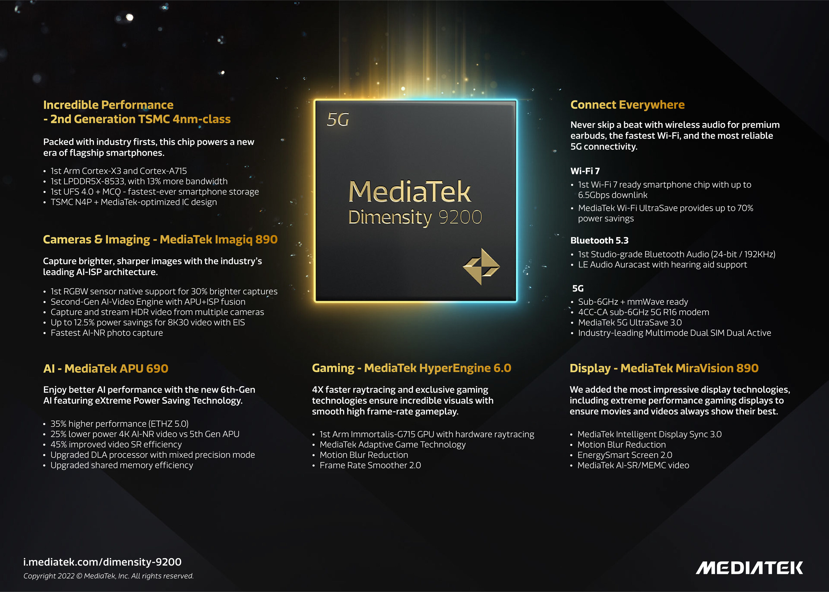
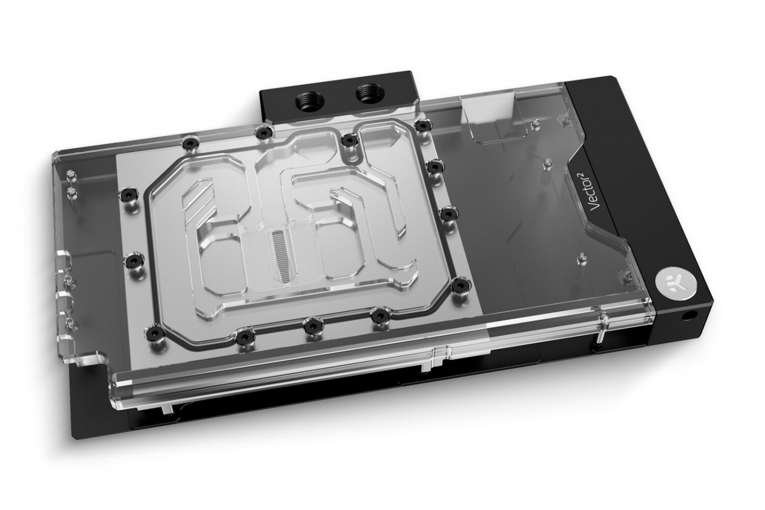
MediaTek Launches Flagship Dimensity 9200 Chipset for Incredible Performance and Unmatched Power Saving

MediaTek today launched the Dimensity 9200, its latest 5G chipset powering the next era of flagship smartphones. Boasting extreme performance and intelligent power efficiency, the new SoC brings immersive all-day gaming experiences, ultra-sharp image capturing and support for both mmWave 5G and sub-6 GHz connectivity to consumers around the globe.

"MediaTek's Dimensity 9200 combines ultimate performance with significant power savings, extending battery life and keeping smartphones cool," said JC Hsu, Corporate Vice President and General Manager of MediaTek's wireless communications business unit at MediaTek. "With notably brighter image capturing and improved gaming speeds, along with the latest display enhancements, the Dimensity 9200 will bring new possibilities for next-gen smartphones that come in a variety of stylish and foldable form factors."

EK Announces Water Blocks for GIGABYTE RTX 4090 AORUS Master and Gaming OC

EK, the premium liquid cooling gear manufacturer, is launching a specialized water block that fits two distinct GPUs from Gigabyte - Aorus GeForce RTX 4090 Master and Gigabyte GeForce RTX 4090 GAMING. EK-Quantum Vector² Master RTX 4090 D-RGB comes in the form of a water block with a passive backplate. The all-new Aorus RTX 4090 Master and Gigabyte RTX 4090 Gaming cards are expected to be significantly more powerful than their 40-series counterparts. And while their efficiency is also improved, these cards still pull over 450 W, which means they will benefit even more from water cooling, mainly due to the 4 nm production process, which increases thermal density compared to the previous 8 nm chips. To top it off, the Master is a behemoth of a card, and opting for water cooling instead of the factory-mounted air cooler, allows you to shrink it several times in the thickness department.

The EK-Quantum Vector² Master RTX 4090 is a single-package liquid cooling solution consisting of a Vector² series water block and black-anodized aluminium backplate. As with the previous 30-series Vector² water blocks, its aesthetics are dominated by minimalist straight lines and the backplate coming around the side of the GPU to cover the PCB completely.

EK Rolls Out New Water Blocks with Active- and Passive-Backplates for RTX 4090 ROG Strix and TUF Gaming

EK, the premium liquid cooling gear manufacturer, is now introducing the ultimate water cooling solution for ROG Strix and ASUS TUF GeForce RTX 4090 graphics cards. EK-Quantum Vector² Strix/TUF RTX 4090 D-RGB comes in the form of a water block with a passive backplate or a cooling solution with an active backplate that's sandwiching the card between two water blocks for the best possible cooling results.

The all-new RTX 4090 Strix and TUF cards are expected to be significantly more powerful than their 30-series counterparts. And while their efficiency is also improved, these cards still pull over 450 W, which means they will benefit even more from water cooling, mainly due to the 4 nm production process, which increases thermal density compared to the previous 8 nm chips.

Samsung Electronics Unveils Plans for 1.4 nm Process Technology

Samsung Electronics, a world leader in advanced semiconductor technology, announced today a strengthened business strategy for its Foundry Business with the introduction of cutting-edge technologies at its annual Samsung Foundry Forum event. With significant market growth in high-performance computing (HPC), artificial intelligence (AI), 5/6G connectivity and automotive applications, demand for advanced semiconductors has increased dramatically, making innovation in semiconductor process technology critical to the business success of foundry customers. To that end, Samsung highlighted its commitment to bringing its most advanced process technology, 1.4-nanometer (nm), for mass production in 2027.

During the event, Samsung also outlined steps its Foundry Business is taking in order to meet customers' needs, including: foundry process technology innovation, process technology optimization for each specific applications, stable production capabilities, and customized services for customers. "The technology development goal down to 1.4 nm and foundry platforms specialized for each application, together with stable supply through consistent investment are all part of Samsung's strategies to secure customers' trust and support their success," said Dr. Si-young Choi, president and head of Foundry Business at Samsung Electronics. "Realizing every customer's innovations with our partners has been at the core of our foundry service."

NVIDIA AD103 and AD104 Chips Powering RTX 4080 Series Detailed

Here's our first look at the "AD103" and "AD104" chips powering the GeForce RTX 4080 16 GB and RTX 4080 12 GB, respectively, thanks to Ryan Smith from Anandtech. These are the second- and third-largest implementations of the GeForce "Ada" graphics architecture, with the "AD102" powering the RTX 4090 being the largest. Both chips are built on the same TSMC 4N (4 nm EUV) silicon fabrication process as the AD102, but are significantly distant from it in specifications. For example, the AD102 has a staggering 80 percent more number-crunching machinery than the AD103, and a 50 percent wider memory interface. The sheer numbers at play here, enable NVIDIA to carve out dozens of SKUs based on the three chips alone, before we're shown the mid-range "AD106" in the future.

The AD103 die measures 378.6 mm², significantly smaller than the 608 mm² of the AD102, and it reflects in a much lower transistor count of 45.9 billion. The chip physically features 80 streaming multiprocessors (SM), which work out to 10,240 CUDA cores, 320 Tensor cores, 80 RT cores, and 320 TMUs. The chip is endowed with a healthy ROP count of 112, and has a 256-bit wide GDDR6X memory interface. The AD104 is smaller still, with a die-size of 294.5 mm², a transistor count of 35.8 billion, 60 SM, 7,680 CUDA cores, 240 Tensor cores, 60 RT cores, 240 TMUs, and 80 ROPs. Ryan Smith says that the RTX 4080 12 GB maxes out the AD104, which means its memory interface is physically just 192-bit wide.

NVIDIA RTX 4090 Doesn't Max-Out AD102, Ample Room Left for Future RTX 4090 Ti

The AD102 silicon on which NVIDIA's new flagship graphics card, the GeForce RTX 4090, is based, is a marvel of semiconductor engineering. Built on the 4 nm EUV (TSMC 4N) silicon fabrication process, the chip has a gargantuan transistor-count of 76.3 billion, a nearly 170% increase over the previous GA102, and a die-size of 608 mm², which is in fact smaller than the 628 mm² die-area of the GA102. This is thanks to TSMC 4N offering nearly thrice the transistor-density of the Samsung 8LPP node on which the GA102 is based.

The AD102 physically features 18,432 CUDA cores, 568 fourth-generation Tensor cores, and 142 third-generation RT cores. The streaming multiprocessors (SM) come with special components that enable the Shader Execution Reordering optimization, which has a significant performance impact on both raster- and ray traced graphics rendering performance. The silicon supports up to 24 GB of GDDR6X or up to 48 GB of GDDR6+ECC memory (the latter will be seen in the RTX Ada professional-visualization card), across a 384-bit wide memory bus. There are 568 TMUs, and a mammoth 192 ROPs on the silicon.

AMD Confirms Optical-Shrink of Zen 4 to the 4nm Node in its Latest Roadmap

AMD in its Ryzen 7000 series launch event shared its near-future CPU architecture roadmap, in which it confirmed that the "Zen 4" microarchitecture, currently on the 5 nm foundry node, will see an optical-shrink to the 4 nm process in the near future. This doesn't necessarily indicate a new-generation CCD (CPU complex die) on 4 nm, it could even be a monolithic mobile SoC on 4 nm, or perhaps even "Zen 4c" (high core-count, low clock-speed, for cloud-compute); but it doesn't rule out the possibility of a 4 nm CCD that the company can use across both its enterprise and client processors.

The last time AMD hyphenated two foundry nodes for a single generation of the "Zen" architecture, was with the original (first-generation) "Zen," which debuted on the 14 nm node, but was optically shrunk and refined on the 12 nm node, with the company designating the evolution as "Zen+." The Ryzen 7000-series desktop processors, as well as the upcoming EPYC "Genoa" server processors, will ship with 5 nm CCDs, with AMD ticking it off in its roadmap. Chronologically placed next to it are "Zen 4" with 3D Vertical Cache (3DV Cache), and the "Zen 4c." The company is planning "Zen 4" with 3DV Cache both for its server- and desktop segments. Further down the roadmap, as we approach 2024, we see the company debut the future "Zen 5" architecture on the same 4 nm node, evolving into 3 nm on certain variants.

NVIDIA Grace CPU Specs Remind Us Why Intel Never Shared x86 with the Green Team

NVIDIA designed the Grace CPU, a processor in the classical sense, to replace the Intel Xeon or AMD EPYC processors it was having to cram into its pre-built HPC compute servers for serial-processing roles, and mainly because those half-a-dozen GPU HPC processors need to be interconnected by a CPU. The company studied the CPU-level limitations and bottlenecks not just with I/O, but also the machine-architecture, and realized its compute servers need a CPU purpose-built for the role, with an architecture that's heavily optimized for NVIDIA's APIs. This, the NVIDIA Grace CPU was born.

This is NVIDIA's first outing with a CPU with a processing footprint rivaling server processors from Intel and AMD. Built on the TSMC N4 (4 nm EUV) silicon fabrication process, it is a monolithic chip that's deployed standalone with an H100 HPC processor on a single board that NVIDIA calls a "Superchip." A board with a Grace and an H100, makes up a "Grace Hopper" Superchip. A board with two Grace CPUs makes a Grace CPU Superchip. Each Grace CPU contains a 900 GB/s switching fabric, a coherent interface, which has seven times the bandwidth of PCI-Express 5.0 x16. This is key to connecting the companion H100 processor, or neighboring Superchips on the node, with coherent memory access.

Qualcomm Launches Snapdragon W5+ and W5 Platforms for Next Generation Wearables

Qualcomm Technologies, Inc. today unveiled the latest additions to the company's suite of premium wearable platforms, Snapdragon W5+ Gen 1 and Snapdragon W5 Gen 1. These platforms are designed to advance ultra-low power and breakthrough performance for next generation connected wearables with a focus on extended battery life, premium user experiences, and sleek, innovative designs. By using these platforms, manufacturers can scale, differentiate, and develop products faster in the continuously growing and segmenting wearables industry.

New enhancements to the flagship Snapdragon W5+ platform offer 50% lower power, 2X higher performance, 2X richer features, and 30% smaller size, compared to our previous generation, enabling wearable manufacturers to deliver the differentiated experiences consumers demand. Based on the hybrid architecture, the purpose-built platform is comprised of a 4 nm-based system-on-chip and 22 nm-based highly integrated always-on co-processor. It incorporates a series of platform innovations including new ultra-low power Bluetooth 5.3 architecture, low power islands for Wi-Fi, GNSS, and Audio, and low power states such as Deep Sleep and Hibernate.

Semiconductor Fab Order Cancellations Expected to Result in Reduced Capacity Utilization Rate in 2H22

According to TrendForce investigations, foundries have seen a wave of order cancellations with the first of these revisions originating from large-size Driver IC and TDDI, which rely on mainstream 0.1X μm and 55 nm processes, respectively. Although products such as MCU and PMIC were previously in short supply, foundries' capacity utilization rate remained roughly at full capacity through their adjustment of product mix. However, a recent wave cancellations have emerged for PMIC, CIS, and certain MCU and SoC orders. Although still dominated by consumer applications, foundries are beginning to feel the strain of the copious order cancellations from customers and capacity utilization rate has officially declined.

Looking at trends in 2H22, TrendForce indicates, in addition to no relief from the sustained downgrade of driver IC demand, inventory adjustment has begun for smartphones, PCs, and TV-related peripheral components such as SoCs, CIS, and PMICs, and companies are beginning to curtail their wafer input plans with foundries. This phenomenon of order cancellations is occurring simultaneously in 8-inch and 12-inch fabs at nodes including 0.1X μm, 90/55 nm, and 40/28 nm. Not even the advanced 7/6 nm processes are immune.

MediaTek Expands Flagship Smartphone Performance with the Dimensity 9000+

MediaTek today announced the Dimensity 9000+, an enhancement to the company's top-of-the-line 5G smartphone chipset. This new high-end offering delivers a boost in performance over the Dimensity 9000 to make the next generation of flagship smartphones even more powerful and efficient.

The new Dimensity 9000+ system-on-chip (SoC) integrates Arm's v9 CPU architecture with a 4 nm octa-core process, combining one ultra-Cortex-X2 core operating at up to 3.20 GHz (compared to 3.05 GHz with the Dimensity 9000) with three super Cortex-A710 cores and four efficiency Cortex-A510 cores. The advanced CPU architecture and Arm Mali-G710 MC10 graphics processor built into the new chipset provide more than a 5% boost in CPU performance and more than 10% improvement in GPU performance.

Off-season Offsets Wafer Pricing Increase, 1Q22 Foundry Output Value Up 8.2% QoQ, Says TrendForce

According to TrendForce research, although demand for consumer electronics remains weak, structural growth demand in the semiconductor industry including for servers, high-performance computing, automotive, and industrial equipment has not flagged, becoming a key driver for medium and long term foundry growth. At the same time, due to robust wafer production at higher pricing in 1Q22, quarterly output value hit a new high for the 11th consecutive quarter, reaching US$31.96 billion, 8.2% QoQ, marginally less than the previous quarter. In terms of ranking, the biggest change is Nexchip surpassed Tower at the ninth position.

TSMC's across the board wafer hikes in 4Q21 on batches primarily produced in 1Q22 coupled with sustained strong demand for high-performance computing and better foreign currency exchange rates pushed TSMC's 1Q22 revenue to $17.53 billion, up 11.3% QoQ. Quarterly revenue growth by node was generally around 10% and the 7/6 nm and 16/12 nm processes posted the highest growth rate due to small expansions in production. The only instance of revenue decline came at the 5/4 nm process due to Apple's iPhone 13 entering the off season for production stocking.

AMD's Second Socket AM5 Ryzen Processor will be "Granite Ridge," Company Announces "Phoenix Point"

AMD in its 2022 Financial Analyst Day presentation announced the codename for the second generation of Ryzen desktop processors for Socket AM5, which is "Granite Ridge." A successor to the Ryzen 7000 "Raphael," the next-generation "Granite Ridge" processor will incorporate the "Zen 5" CPU microarchitecture, with its CPU complex dies (CCDs) built on the 4 nm silicon fabrication node. "Zen 5" will feature several core-level designs as detailed in our older article, including a redesigned front-end with greater parallelism, which should indicate a much large execution stage. The architecture could also incorporate AI/ML performance enhancements as AMD taps into Xilinx IP to add more fixed-function hardware backing the AI/ML capabilities of its processors.

The "Zen 5" microarchitecture makes its client debut with Ryzen "Granite Ridge," and server debut with EPYC "Turin." It's being speculated that AMD could give "Turin" a round of CPU core-count increases, while retaining the same SP5 infrastructure; which means we could see either smaller CCDs, or higher core-count per CCD with "Zen 5." Much like "Raphael," the next-gen "Granite Ridge" will be a series of high core-count desktop processors that will feature a functional iGPU that's good enough for desktop/productivity, though not gaming. AMD confirmed that it doesn't see "Raphael" as an APU, and that its definition of an "APU" is a processor with a large iGPU that's capable of gaming. The company's next such APU will be "Phoenix Point."

AMD Announces the "Zen 5" Microarchitecture and EPYC "Turin" Processor on 4nm

AMD in its Financial Analyst Day 2022 presentation, unveiled its next-generation "Zen 5" CPU microarchitecture. The company's latest CPU microarchitecture roadmap also confirms that variants of its "Zen 4" CCDs with 3D Vertical Cache (3DV Cache) are very much in the works, and there will be variants of the EPYC "Genoa" processors with 3DV Cache, besides standard ones.

AMD stated that it completed the design goal of the current "Zen 3" architecture, by building it on both 7 nm and 6 nm nodes (the latter being the client "Rembrandt" processor). The new "Zen 4" architecture will debut on the 5 nm node (TSMC N5), and could see a similar optical shrink to the newer 4 nm node somewhere down the line, although AMD wouldn't specify whether it's on the enterprise segment, or client. The next-gen "Zen 5" architecture will debut on 4 nm, and see an optical shrink to 3 nm on some future product.

After TSMC, Intel May be Edging Closer to Samsung for Collaboration

Intel's revamped IDM 2.0 strategy has seen the company revise its stance in both in-house and outsourced silicon fabrication. While we're already seeing the fruits of Intel's collaboration with TSMC (albeit at the relatively slow pace of introduction for Intel's Arc Alchemist graphics), it seems that Intel is willing to go much farther than just TSMC as a source of chips for its product portfolio.

That's the backdrop to which Intel CEO Pat Gelsinger recently took a trip to South Korea's capital of Seoul. According to the Korea Herald, Gelsinger met several key Samsung executives, including Samsung Electronics Vice Chairman Lee Jae-yong, co-CEO and chip business boss Kyung Kye-hyun, and head of Samsung Mobile Roh Tae-moon. More than enough executive grunt to ignite talks of a deepening collaboration between both companies. While the reporting source doesn't provide any quotes or actionable intel from the meeting, Samsung remains one of the key semiconductor manufacturers alongside Intel itself and TSMC, with a particularly strong portfolio in memory-related technologies.

Samsung Foundry Considering up to 20 Percent Price Hikes

Earlier this week, news about TSMC increasing prices in 2023 made its way online and now Samsung Foundry is said to be discussing price hikes with its customers to make up for the increased costs in materials. TSMC already increased its prices by around 20 percent at the end of 2021 and now it looks like Samsung Foundry is set to follow suit with a similar price hike. Depending on the node, the company is said to be looking at increases of between 15 to 20 percent. The somewhat peculiar thing in the case of Samsung Foundry, is that the company is looking at asking for more money on older, legacy nodes, than it will for its cutting edge nodes.

The price increases are said to come into effect sometime in the second half of 2022, so more than six months after TSMC's price hike. The company is still in negotiation with some of its customers, while others have already come to an agreement with Samsung Foundries. The costs to produce chips are said to be increasing by 20 to 30 percent across the board, no matter if we're talking materials needed to produce integrated circuits, or building new factories, according to Bloomberg. Samsung Foundries have also managed to secure long-term orders for the next five years, with a combined value of around eight times that of previous year's revenue, according to its EVP, Kang Moon-soo. The company is hoping to overtake TSMC in the future and invested more than US$36 billion in 2021 alone to expand its foundry business with new fabs and EUV machines. The good news is that Samsung Foundry claims to be back on track when it comes to yield on its 4 nm node and mass production of its 3 nm node is said to start this quarter.

NVIDIA H100 SXM Hopper GPU Pictured Up Close

ServeTheHome, a tech media outlet focused on everything server/enterprise, posted an exclusive set of photos of NVIDIA's latest H100 "Hopper" accelerator. Being the fastest GPU NVIDIA ever created, H100 is made on TSMC's 4 nm manufacturing process and features over 80 billion transistors on an 814 mm² CoWoS package designed by TSMC. Complementing the massive die, we have 80 GB of HBM3 memory that sits close to the die. Pictured below, we have an SXM5 H100 module packed with VRM and power regulation. Given that the rated TDP for this GPU is 700 Watts, power regulation is a serious concern and NVIDIA managed to keep it in check.

On the back of the card, we see one short and one longer mezzanine connector that acts as a power delivery connector, different from the previous A100 GPU layout. This board model is labeled PG520 and is very close to the official renders that NVIDIA supplied us with on launch day.

NVIDIA Hopper Whitepaper Reveals Key Specs of Monstrous Compute Processor

The NVIDIA GH100 silicon powering the next-generation NVIDIA H100 compute processor is a monstrosity on paper, with an NVIDIA whitepaper published over the weekend revealing its key specifications. NVIDIA is tapping into the most advanced silicon fabrication node currently available from TSMC to build the compute die, which is TSMC N4 (4 nm-class EUV). The H100 features a monolithic silicon surrounded by up to six on-package HBM3 stacks.

The GH100 compute die is built on the 4 nm EUV process, and has a monstrous transistor-count of 80 billion, a nearly 50% increase over the GA100. Interestingly though, at 814 mm², the die-area of the GH100 is less than that of the GA100, with its 826 mm² die built on the 7 nm DUV (TSMC N7) node, all thanks to the transistor-density gains of the 4 nm node over the 7 nm one.

Samsung Says Future Fab Nodes Are On Time, no Yield Issues on Current Nodes

Despite rumours of both production issues and node delays, Samsung has assured its shareholders during its first quarter conference call, that the company is on track. Its yield rate from its 5 nm node was said to have entered maturity, meaning that yields have entered Samsung's expected levels. However, Samsung did admit that its 4 nm node had seen some delays with the ramp up, but it has now entered the expected yield rate curve. The company is also working on an new R&D line for its upcoming 3 nm node, but didn't go into any further details.

As for Samsung's DRAM products, there were rumours that its 12 nm 1b process node had hit some snags and that the company was going to skip ahead to its 1c node, something the company denied. Samsung added that the development of 1b was proceeding stably and that the 1c node is expected to be done on schedule. The company also said that media reports of issues at Samsung's foundry business were overblown and that order books are full, which is why some of its customers have had to produce additional parts with TSMC. Samsung's foundry business reportedly saw an increase in operating profit of 50 percent compared to last year, as well as an increase in revenue of 19 percent.

TSMC Ramps up Shipments to Record Levels, 5/4 nm Production Lines at Capacity

According to DigiTimes, TSMC is working on increased its monthly shipments of finished wafers from 120,000 to 150,000 for its 5 nm nodes, under which 4 nm also falls. This is three times as much as what TSMC was producing just a year ago. The 4 nm node is said to be in full mass production now and the enhanced N4P node should be ready for mass production in the second half of 2022, alongside N3B. This will be followed by the N4X and N3E nodes in 2023. The N3B node is expected to hit 40-50,000 wafers initially, before ramping up from there, assuming everything is on track.

The report also mentions that TSMC is expecting a 20 percent revenue increase from its 28 to 7 nm nodes this year, which shows that even these older nodes are being heavily utilised by its customers. TSMC has what NVIDIA would call a demand problem, as the company simply can't meet demand at the moment, with customers lining up to be able to get a share of any additional production capacity. NVIDIA is said to have paid TSMC at least US$10 billion in advance to secure manufacturing capacity for its upcoming products, both for consumer and enterprise products. TSMC's top three HPC customers are also said to have pre-booked capacity on the upcoming 3 and 2 nm nodes, so it doesn't look like demand is going to ease up anytime soon.

Qualcomm Said to be Moving to TSMC for 3 nm Chips

Although nothing has been officially confirmed by Qualcomm, it looks like the company will be moving away from Samsung for its 3 nm based chips, in favour of TSMC. The Elec also mentions that Qualcomm has moved some of its Snapdragon 8 Gen 1 production to TSMC, something that has already been hitting the rumour mill. The first batch of 4 nm Snapdragon 8 Gen 1 chips are said to already have entered the early stages of production. The main reason for the move is said to be poor yields by Samsung Foundry on its 4 nm node.

The yield rates are said to be a measly 35 percent for the Snapdragon 8 Gen 1, with Samsung's Exynos 2200 having even lower yields. This also helps explain why Samsung's mobile division has decided to limit the availability of its Exynos 2200 based phones to only a few regions. Apparently Qualcomm had to send staff over to Korea to help get the yields up to their current rate, but it's not hard to see why the company is shifting back to TSMC, as a 35 percent yield rate is simply not acceptable. Samsung is said to be auditing Samsung Foundry to find out what has gone wrong, as anything below 80-90 percent in terms of yield rate is simply not acceptable for mass production. Qualcomm will apparently continue to use Samsung Foundry for its 7 nm RF chips, where the yields must be within industry norms.

Samsung Employees Being Investigated for "Fabricating" Yields

Samsung Electronics is hit by a major scandal involving current and former employees. It's being alleged that these employees are involved in falsifying information about the semiconductor fabrication yields of the company's 3/4/5 nanometer nodes to clear them for commercial activity. This came to light when Samsung was observing lower than expected yields after the nodes were approved for mass-production of logic chips for Samsung, as well as third-party chip-designers. A falsified yield figure can have a cascading impact across the supply-chain, as wafer orders and pricing are decided on the basis of yields. Samsung however, has downplayed the severity of the matter. The group has initiated an investigation into Samsung Device Solutions, the business responsible for the foundry arm of the company. This includes a thorough financial audit of the foundry to investigate if the investments made to improve yields were properly used.

TSMC Announces the N4X Silicon Fabrication Process

TSMC today introduced its N4X process technology, tailored for the demanding workloads of high performance computing (HPC) products. N4X is the first of TSMC's HPC-focused technology offerings, representing ultimate performance and maximum clock frequencies in the 5-nanometer family. The "X" designation is reserved for TSMC technologies that are developed specifically for HPC products.

"HPC is now TSMC's fastest-growing business segment and we are proud to introduce N4X, the first in the 'X' lineage of our extreme performance semiconductor technologies," said Dr. Kevin Zhang, senior vice president of Business Development at TSMC. "The demands of the HPC segment are unrelenting, and TSMC has not only tailored our 'X' semiconductor technologies to unleash ultimate performance but has also combined it with our 3DFabric advanced packaging technologies to offer the best HPC platform."

AMD to Tap Samsung's 4 nm Process for Chromebook Processors, Notes the Report from J.P. Morgan

Historically, AMD was working with two semiconductor manufacturing companies: TSMC and GlobalFoundries. According to the latest report coming from Gokul Hariharan, an analyst at J.P. Morgan, AMD could soon tap another semiconductor manufacturer to produce the company's growing list of processors. As the report indicates, AMD could start working with the South Korean giant Samsung and utilize the firm's 4LPP process that represents a second generation of the low-power 4 nm silicon node. This specific node is allegedly the choice for AMD APUs designed to fit inside Google's Chromebook devices, which require low-power designs to achieve excellent battery life.

AMD could realize this move in late 2022, as Samsung's 4LPP node goes into mass production at that point. It means that we could see the first Samsung-made AMD APUs in late 2022 or the beginning of 2023. And apparently, the two company's collaboration could be much more significant as AMD is evaluating Samsung's 3 nm nodes for other products spanning more segments in 2023/2024. There are no official, definitive agreements between the two, so we have to wait for more information and official responses from these parties. Anyways, if AMD decides to produce a part of its lineup at Samsung, the remaining TSMC capacity would ensure that the supply of every incoming chip remains sufficient.

Qualcomm CEO Expects Chip Shortage To Ease in 2022

Qualcomm CEO Cristiano Amon has claimed that the global chip shortage is easing with the situation expected to improve further in 2022. The availability of chips in 2022 should be significantly improved compared to 2020 Cristiano Amon told reporters in South Korea on Thursday. Qualcomm has struggled to meet the demand for its smartphone processors which has resulted in reduced smartphone production. The next-generation Qualcomm Snapdragon 8 Gen 1 processor recently announced by the company will be manufactured on Samsung Foundry's 4 nm node with the yield rate ultimately determining Qualcomm's ability to meet demand in 2022. This prediction is slightly more optimistic than other companies including Intel and IBM who don't expect the shortage to be resolved until 2023.
Return to Keyword Browsing
Jul 24th, 2025 19:07 CDT change timezone

New Forum Posts

Popular Reviews

TPU on YouTube

Controversial News Posts