News Posts matching #5 nm

Return to Keyword Browsing

MediaTek Announces Dimensity 8050 SoC, Seems to be a Rebadged Dimensity 1300/1200

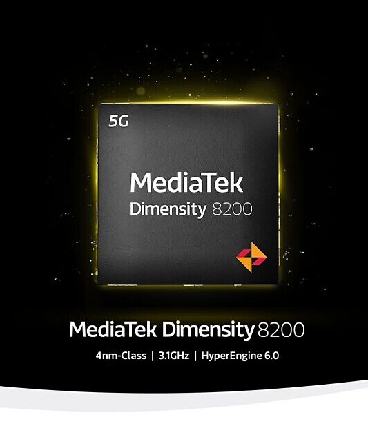
MediaTek has been unveiling some new mobile chipsets this week, but keen-eyed news outlets have noticed that the Taiwanese fabless semiconductor company is simply renaming and relaunching hardware from last year, with some tweaks here and there. Today's announcement of the Dimensity 8050 SoC was almost immediately questioned - GSMArena noticed that this "new" model was a near dead ringer, in terms of specifications, for last year's mid-range Dimensity 1300 and 1200 smartphone chipsets. There are some upgrades in terms of memory bandwidth, and MediaTek boasts that the 8050 has been updated with its sixth generation HyperEngine technology.

Alarm bells were ringing when folks realized that the much older Dimensity 8000 SoC was built on a 5 nm process - the supposedly superior (in terms of model number hierarchy) 8005 is a 6 nm chip. Last week the mobile specialist site also spotted that MediaTek's Dimensity 7050 chipset was yet another example of the smartphone tech company rolling out a "rebranding phase." The news outlet pointed out that this newly revealed mobile CPU was just a renamed Dimensity 1080 - with the original model having hit the market in November 2022. MediaTek seems to renaming several older chipsets based on TSMC's 6 nm process - it is possible that this effort is part of a company drive to clear surplus silicon.

NVIDIA GeForce RTX 4060 Ti Available as 8 GB and 16 GB, This Month. RTX 4060 in July

In what could explain the greater attention by leaky taps on the GeForce RTX 4060 Ti compared to its sibling, the RTX 4060, NVIDIA is preparing a staggered launch for its RTX 4060-series. We're also learning that there are as many as three SKUs in the series—the RTX 4060 Ti 8 GB, the RTX 4060 Ti 16 GB, and the RTX 4060. All three will be announced later this month, however, only the RTX 4060 Ti 8 GB will be available to purchase at the time. The RTX 4060 Ti 16 GB and RTX 4060 will be available from July.

At this point, little is known about what segments the 8 GB and 16 GB variants of the RTX 4060 Ti besides memory size. The RTX 4060 Ti 8 GB is rumored to feature 34 out of 36 streaming multiprocessors (SM) physically present on the 5 nm "AD106" silicon, which gives NVIDIA some theoretical headroom to enable a few more shaders. These 34 work out to 4,352 CUDA cores, while a fully unlocked AD106 has 4,608. The RTX 4060 is a significantly different SKU that's based on a maxed out "AD107" silicon, with 30 SM, or 3,840 CUDA cores, although it should be possible for some RTX 4060 cards be based on a heavily cut-down AD106.

SK Hynix to Expand Wuxi Fab Legacy Production Capacity, Consumer DRAM Prices Struggle to Recover

Last October, the US Department of Commerce imposed semiconductor restrictions on Chinese imports of equipment for processes of 18 nm and below. SK hynix's Wuxi fab was granted a one-year production license, but geopolitical risks and weak demand prompted the company to reduce wafer starts by about 30% per month in 2Q23, according to TrendForce's latest research.

TrendForce reports that SK hynix had planned to transition its Wuxi fab's mainstream process from 1Y nm to 1Z nm, decreasing the output of legacy processes. However, due to limitations imposed by the US ban, the company instead opted to increase the share of its 21 nm production lines, focus-ing on DDR3 and DDR4 4Gb products. SK hynix's long-term strategy involves shifting its capacity expansion back to South Korea, while the Wuxi fab caters to domestic demand in China and the legacy-process consumer DRAM market.

AMD Radeon RX 7600 XT Launches on May 25

AMD Radeon RX 7600 XT reportedly launches on May 25, 2023. Moore's Law is Dead scored the key dates associated with the launch. The upcoming performance-segment graphics card is rumored to be based on the 5 nm "Navi 33" silicon and RDNA3 graphics architecture. Apparently, the tech press should have its samples to test by May 15, and AMD is taking a similar approach to NVIDIA's recent GeForce RTX 4070 launch, where cards priced at MSRP will be eligible to a review embargo that's a day sooner than that of non-MSRP cards. Reviews of MSRP cards go live on May 24, with those of non-MSRP cards following the next day on May 25, along with market availability. It's no wonder that we heard reports of RX 7600 series cards being shown off at Computex, all those cards will be available to purchase by then.

AMD Radeon RX 7600 Early Sample Offers RX 6750 XT Performance at 175W: Rumor

AMD is expected to debut its performance-segment Radeon RX 7600 RDNA3 graphics card in May-June 2023, with board partners expected to show off their custom-design cards in the 2023 Computex (June). Moore's Law is Dead reports that they've spoken to a source with access to an early graphics card sample running the 5 nm "Navi 33" silicon that powers the RX 7600. This card, with development drivers (which are sure to be riddled with performance limiters); offers a 11% performance uplift over the Radeon RX 6650 XT, and a gaming power draw of 175 W (the RX 6650 XT pulls around 185-190 W).

This is still an early sample running development drivers, but a 11% performance boost puts it in the league of the Radeon RX 6700 XT. Should a production RX 7600 with launch-day drivers put on another 5-7% performance over this, the RX 7600 could end up with performance roughly matching the RX 6750 XT (a slim performance lead over the RTX 3070 in 1080p gaming). Should its power draw also hold, one can expect custom-design graphics cards to ship with single 8-pin PCIe power connectors. A couple of nifty specs of the RX 7600 also leaked out in the MLID report: Firstly, that 8 GB will remain the standard memory size for the RX 7600, as it is for the current RX 6650 XT. Secondly, the RX 7600 engine clock is reported to boost "above" 2.60 GHz.

Synopsys, TSMC and Ansys Strengthen Ecosystem Collaboration to Advance Multi-Die Systems

Accelerating the integration of heterogeneous dies to enable the next level of system scalability and functionality, Synopsys, Inc. (Nasdaq: SNPS) has strengthened its collaboration with TSMC and Ansys for multi-die system design and manufacturing. Synopsys provides the industry's most comprehensive EDA and IP solutions for multi-die systems on TSMC's advanced 7 nm, 5 nm and 3 nm process technologies with support for TSMC 3DFabric technologies and 3Dblox standard. The integration of Synopsys implementation and signoff solutions and Ansys multi-physics analysis technology on TSMC processes allows designers to tackle the biggest challenges of multi-die systems, from early exploration to architecture design with signoff power, signal and thermal integrity analysis.

"Multi-die systems provide a way forward to achieve reduced power and area and higher performance, opening the door to a new era of innovation at the system-level," said Dan Kochpatcharin, head of Design Infrastructure Management Division at TSMC. "Our long-standing collaboration with Open Innovation Platform (OIP) ecosystem partners like Synopsys and Ansys gives mutual customers a faster path to multi-die system success through a full spectrum of best-in-class EDA and IP solutions optimized for our most advanced technologies."

Microsoft Working on Custom AI Processor Codenamed Project Athena

According to The Information, Microsoft has been working on creating custom processors for processing AI with a project codenamed Athena. Based on TSMC's 5 nm process, these chips are designed to accelerate AI workloads and scale to hundreds or even thousands of chips. With the boom of Large Language Models (LLMs) that require billions of parameters, training them requires a rapid increase of computational power to a point where companies purchase hundreds of thousands of GPUs from the likes of NVIDIA. However, creating custom processors is a familiar feat for a company like Microsoft. Hyperscalers like AWS, Google, and Meta are already invested in the creation of processors for AI training, and Microsoft is just joining as well.

While we don't have much information about these processors, we know that Microsoft started the project in 2019, and today these processors are in the hands of select employees of Microsoft and OpenAI that work with AI projects and need computational horsepower. Interestingly, some projections assume that if Microsoft could match NVIDIA's GPU performance, the cost would only be a third of NVIDIA's offerings. However, it is challenging to predict that until more information is provided. Microsoft plans to make these chips more widely available as early as next year; however, there is no specific information on when and how, but Azure cloud customers would be the most logical place to start.

AMD 96-Core EPYC 9684X Zen 4 Genoa-X CPU Shows Up for Sale in China

The second-hand market in China is always full of gems, but we never expected to see an unreleased 5 nm 96-core EPYC 9684X Genoa-X CPU with 1152 MB of L3 cache. According to the seller, the CPU is "almost new" and in working condition.

In case you missed it earlier, AMD is working on 5 nm Genoa-X EPYC CPUs which will feature up to 96 Zen 4 cores in 5 nm with over 1 GB of L3 cache per socket. These are scheduled to release this year, optimized for technical computing and databases. AMD is also working on Siena CPUs, which should also come this year, featuring up to 64 Zen 4 cores with optimized performance-per-watt, meant for intelligent edge and telco markets.

AMD Introduces Alveo MA35D Media Accelerator

AMD today announced the AMD Alveo MA35D media accelerator featuring two 5 nm, ASIC-based video processing units (VPUs) supporting the AV1 compression standard and purpose-built to power a new era of live interactive streaming services at scale. With over 70% of the global video market being dominated by live content, a new class of low-latency, high-volume interactive streaming applications are emerging such as watch parties, live shopping, online auctions, and social streaming.

The Alveo MA35D media accelerator delivers the high channel density, with up to 32x 1080p60 streams per card, power efficiency and ultra-low-latency performance critical to reducing the skyrocketing infrastructure costs now required for scaling such compute intensive content delivery. Compared to the previous generation Alveo U30 media accelerator, the Alveo MA35D delivers up to 4x higher channel density, 4x max lower latency in 4K and 1.8x greater compression efficiency to achieve the same VMAF score—a common video quality metric.

NVIDIA GeForce RTX 4050 "Ada" Launches This June

NVIDIA's mainstream GeForce RTX 4050 "Ada" graphics card, which succeeds the RTX 3050, reportedly launches in June 2023. This could end up being the highest-volume SKU in the RTX 40-series desktop lineup. Team green is planning to launch a new desktop SKU every month leading up to Summer. April will see the company launch the performance-segment RTX 4070, followed by the RTX 4060 Ti and RTX 4060 in May, and now we hear about the RTX 4050 in June.

The GeForce RTX 4050 is likely based on a highly cut down version of the 5 nm "AD107" silicon that also powers the RTX 4060 in its maxed out configuration. The AD107, much like the AD106, features a 128-bit wide GDDR6 memory interface. For the RTX 4050, NVIDIA could narrow this down to 96-bit, and give it 6 GB of GDDR6 memory, which is 25% less than the 8 GB of 128-bit GDDR6 memory that's standard for the current-generation RTX 3050. NVIDIA would have worked out the performance numbers, and the RTX 4050 might still end up generationally faster than the RTX 3050 despite this narrower/smaller memory.

TSMC's 3 nm Node at Near 50 Percent Utilisation, Other Nodes Seeing Lower Demand

Based on multiple reports out of Taiwan, TSMC is seeing increased utilisation of its 3 nm node and its production line is now at close to 50 percent utilisation. The main customer here is without a doubt Apple and TSMC is churning out some 50-55,000 wafers a month on its 3 nm node. TSMC is also getting ready to start production on its N3E node later this year, which will see some customers move to the node.

However, it's not all good news, as TSMC is seeing a decline in utilisation on its 5/4 and 7/6 nm nodes as demand has dropped significantly here, with different news outlets reporting different figures. Some are suggesting the 7/6 nm nodes might have dropped as low as to 50 percent utilisation, others mention 70 percent. The 5/4 nm nodes aren't anywhere nearly as badly affected and remain at around 80 percent utilisation. The good news for TSMC is that this is expected to be a temporary slump in demand and most of its leading edge nodes should be back at somewhere around a 90 percent utilisation rate by the second half of the year. However, this depends on what the demand for its partners' products will look like going forward, as many of TSMC's customers are seeing lower demand for their products in turn.

AMD Ryzen 7045HX3D "Dragon Range" with 3DV Cache Should Technically be Possible

There are two distinct developments in the client processor space for AMD—first, its Ryzen 7000X3D desktop processors have managed to retain gaming performance competitiveness against Intel's fastest 13th Gen Core "Raptor Lake" processors; and second, that its Ryzen 7045HX "Dragon Range" mobile processors are picking up interest in the enthusiast-segment notebook community, where its advanced 5 nm + 6 nm process is dealing damage to 13th Gen Core mobile processors in performance/Watt, and gaming performance. Can AMD dial things up a notch? Technically, yes.

It should technically be possible for AMD to build "Dragon Range" multi-chip modules using "Zen 4" + 3D Vertical Cache CCDs (CPU complex dies), much in the same way it did for the desktop product stack. Such a processor would either have one CCD with the 3DV cache for a CPU core-count of up to 8-core/16-thread; or a contraption similar to the desktop 7950X3D, wherein one of the CCDs has 3DV cache, while the other is a regular "Zen 4" CCD, for core-counts of up to 16-core/32-thread. But will AMD build such chips? A lot would depend on the volumes of L3Ds (the 6 nm dies with the 64 MB 3D Vertical cache memory that operates at 2.5 TB/s), the production of CCDs with 3DV cache; and whether AMD is able to achieve the right performance/Watt numbers against Intel's fastest 8P+16E "Raptor Lake" mobile processors.

AMD RDNA4 Architecture to Build on Features Relevant to Gaming Performance, Doesn't Want to be Baited into an AI Feature Competition with NVIDIA

AMD's next-generation RDNA4 graphics architecture will retain a design-focus on gaming performance, without being drawn into an AI feature-set competition with rival NVIDIA. David Wang, SVP Radeon Technologies Group; and Rick Bergman, EVP of Computing and Graphics Business at AMD; gave an interview to Japanese tech publication 4Gamers, in which they dropped the first hints on the direction which the company's next-generation graphics architecture will take.

While acknowledging NVIDIA's movement in the GPU-accelerated AI space, AMD said that it didn't believe that image processing and performance-upscaling is the best use of the AI-compute resources of the GPU, and that the client segment still hasn't found extensive use of GPU-accelerated AI (or for that matter, even CPU-based AI acceleration). AMD's own image processing tech, FSR, doesn't leverage AI acceleration. Wang said that with the company introducing AI acceleration hardware with its RDNA3 architecture, he hopes that AI is leveraged in improving gameplay—such as procedural world generation, NPCs, bot AI, etc; to add the next level of complexity; rather than spending the hardware resources on image-processing.

Intel Meteor Lake to Feature 50% Increase in Efficiency, 2X Faster iGPU

Intel's upcoming Meteor Lake processor family is supposedly looking good with the new performance/efficiency targets. According to the @OneRaichu Twitter account, we have a potential performance estimate for the upcoming SKUs. As the latest information notes, Intel's 14th-generation Meteor Lake will feature around a 50% increase in efficiency compared to the 13th-generation Raptor Lake designs. This means that the processor can use half the power at the same performance target at Raptor Lake, increasing efficiency. Of course, the design also offers some performance improvements besides efficiency that are significant and are yet to be shown. The new Redwood Cove P-cores will be combined with the new Crestmont E-cores for maximum performance inside U/P/H configurations with 15-45 Watt power envelopes.

For integrated graphics, the source notes that Meteor Lake offers twice the performance of iGPU found on Raptor Lake designs. Supposedly, Meteor Lake will feature 128 EUs running 2.0+GHz compared to 96 EUs found inside Raptor Lake. The iGPU architecture will switch from Intel Iris to Xe-LPG 'Xe-MTL' family on the 14th gen models, confirming a giant leap in performance that iGPU is supposed to experience. Using the tile-based design, Intel combines the Intel 4 process for the CPU tile and the TSMC 5 nm process for the GPU tile. Intel handles final packaging for additional tuning, and you can see the separation below.

MSI Radeon RX 7900 XTX Gaming Trio Classic Listed at $1100

MSI Radeon RX 7900 XTX Gaming Trio Classic, the company's first Radeon 7000 series RDNA3 graphics card, is finally listed online. American retailer Newegg put it up for sale at $1,100, a $100 premium over the $1000 AMD baseline price for the RX 7900 XTX. This is a "sold and shipped by Newegg" listing. MSI showed this card off last month, at the 2023 International CES. It pairs a custom-design PCB with a previous-generation Tri Frozr 2.0 cooling solution—the same one it used with its RX 6950 XT Gaming series. The PCB, however, is an MSI in-house design, with a meaty VRM that draws power from three 8-pin PCIe power connectors, and should hence feature a higher power-limit than the reference-design board, which has been known to scoop out a far greater overclocking headroom on other cards with a similar power setup (such as the ASUS TUF Gaming RX 7900 XTX).

The MSI RX 7900 XTX Gaming Trio Classic comes with clock speeds of 2.30 GHz game, and 2.50 GHz boost, which surprisingly are AMD's reference clocks. Perhaps MSI is saving factory-overclocks for the RX 7900 XTX Gaming X Trio Classic, which it will price even higher. Maxing out the 5 nm "Navi 31" GPU, the RX 7900 XTX offers 6,144 stream processors across 96 RDNA3 compute units, with 96 Ray Accelerators, 384 TMUs, 192 ROPs, and a 384-bit wide GDDR6 memory interface, running 24 GB of memory at 20 Gbps (960 GB/s memory bandwidth).

Samsung Electronics Announces Fourth Quarter and FY 2022 Results, Profits at an 8-year Low

Samsung Electronics today reported financial results for the fourth quarter and the fiscal year 2022. The Company posted KRW 70.46 trillion in consolidated revenue and KRW 4.31 trillion in operating profit in the quarter ended December 31, 2022. For the full year, it reported 302.23 trillion in annual revenue, a record high and KRW 43.38 trillion in operating profit.

The business environment deteriorated significantly in the fourth quarter due to weak demand amid a global economic slowdown. Earnings at the Memory Business decreased sharply as prices fell and customers continued to adjust inventory. The System LSI Business also saw a decline in earnings as sales of key products were weighed down by inventory adjustments in the industry. The Foundry Business posted a new record for quarterly revenue while profit increased year-on-year on the back of advanced node capacity expansion as well as customer base and application area diversification.

Foundry Revenue is Forecasted to Drop by 4% YoY for 2023, TrendForce Notes

TrendForce's recent analysis of the foundry market reveals that demand continues to slide for all types of mature and advanced nodes. The major IC design houses have cut wafer input for 1Q23 and will likely scale back further for 2Q23. Currently, foundries are expected to maintain a lower-than-ideal level of capacity utilization rate in the first two quarters of this year. Some nodes could experience a steeper demand drop in 2Q23 as there are still no signs of a significant rebound in wafer orders. Looking ahead to the second half of this year, orders will likely pick up for some components that underwent an inventory correction at an earlier time. However, the state of the global economy will remain the largest variable that affect demand, and the recovery of individual foundries' capacity utilization rates will not occur as quickly as expected. Taking these factors into account, TrendForce currently forecasts that global foundry revenue will drop by around 4% YoY for 2023. The projected decline for 2023 is more severe when compared with the one that was recorded for 2019.

AMD Shows Instinct MI300 Exascale APU with 146 Billion Transistors

During its CES 2023 keynote, AMD announced its latest Instinct MI300 APU, a first of its kind in the data center world. Combining the CPU, GPU, and memory elements into a single package eliminates latency imposed by long travel distances of data from CPU to memory and from CPU to GPU throughout the PCIe connector. In addition to solving some latency issues, less power is needed to move the data and provide greater efficiency. The Instinct MI300 features 24 Zen4 cores with simultaneous multi-threading enabled, CDNA3 GPU IP, and 128 GB of HBM3 memory on a single package. The memory bus is 8192-bit wide, providing unified memory access for CPU and GPU cores. CLX 3.0 is also supported, making cache-coherent interconnecting a reality.

The Instinct MI300 APU package is an engineering marvel of its own, with advanced chiplet techniques used. AMD managed to do 3D stacking and has nine 5 nm logic chiplets that are 3D stacked on top of four 6 nm chiplets with HBM surrounding it. All of this makes the transistor count go up to 146 billion, representing the sheer complexity of a such design. For performance figures, AMD provided a comparison to Instinct MI250X GPU. In raw AI performance, the MI300 features an 8x improvement over MI250X, while the performance-per-watt is "reduced" to a 5x increase. While we do not know what benchmark applications were used, there is a probability that some standard benchmarks like MLPerf were used. For availability, AMD targets the end of 2023, when the "El Capitan" exascale supercomputer will arrive using these Instinct MI300 APU accelerators. Pricing is unknown and will be unveiled to enterprise customers first around launch.

AMD Launches Ryzen 7045HX Series 16-core "Dragon Range" Enthusiast Mobile Processors

AMD today solved the biggest challenge affecting its mobile processor family against Intel—CPU core-counts in the high-end HX-segment, with the introduction of the new Ryzen 7045HX series "Dragon Range" mobile processors. Based on the "Zen 4" microarchitecture, these processors offer core-counts of up to 16-core/32-thread, and target enthusiast gaming notebooks and mobile workstations. The processors debut the new "Dragon Range" multi-chip module (MCM). This is essentially a non-socketed version of the desktop "Raphael" MCM built in a mobile-friendly BGA package with a thin substrate and no IHS, with up to two 5 nm "Zen 4" 8-core CCDs, and a 6 nm cIOD (client I/O die).

The "Dragon Range" MCM uses the same chiplets as desktop "Raphael" Ryzen 7000 processors, and so its I/O is similar. The cIOD puts out a dual-channel (4 sub-channel) DDR5 memory interface, and a PCI-Express 5.0 x16 interface for discrete graphics, along with two PCI-Express 5.0 x4 links for up to two Gen 5 NVMe SSDs. The platform core-logic (chipset) is functionally similar to the desktop AMD B650E. All processor models in the series come with a TDP of 45 W, and a package power tracking (PPT) of "at least" 75 W. Each "Zen 4" CPU core comes with 1 MB of dedicated L2 cache, and each CCD has 32 MB of L3 cache.

Top 10 TSMC Customers Said to have Cut Orders for 2023

On the day of TSMC's celebration of the mass production start of its 3 nm node, news out of Taiwan suggests that all of its top 10 customers have cut their orders for 2023. However, the cuts are unlikely to affect its new node, but rather its existing nodes, with the 7 and 6 nm nodes said to be hit the hardest, by as much as a 50 percent utilisation reduction in the first quarter of 2023. The 28 nm and 5 and 4 nm nodes are also said to be affected, although it's unclear by how much at this point in time.

Revenue is expected to fall by at least 15 percent in the first quarter of 2023 for TSMC, based on numbers from DigiTimes. The fact that TSMC has increased its 2023 pricing by six percent should at least help offset some of the potential losses for the company, but it all depends on the demand for the rest of the year. Demand for mobile devices is down globally, which is part of the reason why so many of TSMC's customers have cut back their orders, as Apple, Qualcomm and Mediatek all produce their mobile SoCs at TSMC. Add to this that the demand for computers and new computer components are also down, largely due to the current pricing and TSMC is in for a tough time next year.

TSMC Holds 3nm Volume Production and Capacity Expansion Ceremony, Marking a Key Milestone for Advanced Manufacturing

TSMC today held a 3 nanometer (3 nm) Volume Production and Capacity Expansion Ceremony at its Fab 18 new construction site in the Southern Taiwan Science Park (STSP), bringing together suppliers, construction partners, central and local government, the Taiwan Semiconductor Industry Association, and members of academia to witness an important milestone in the Company's advanced manufacturing.

TSMC has laid a strong foundation for 3 nm technology and capacity expansion, with Fab 18 located in the STSP serving as the Company's GIGAFAB facility producing 5 nm and 3 nm process technology. Today, TSMC announced that 3 nm technology has successfully entered volume production with good yields, and held a topping ceremony for its Fab 18 Phase 8 facility. TSMC estimates that 3 nm technology will create end products with a market value of US$1.5 trillion within five years of volume production.

TSMC to Mark 3 nm Mass Production Start, Looking at Potential New Fabs in Japan and Germany

According to news out of Taiwan, TSMC will hold a ceremony to mark the official mass production start of its 3 nm node on the 29th of December. This is said to help "shatter doubts about de-Taiwanization" or in simpler terms, that Taiwan will lose its golden goose as TSMC invests abroad. The 3 nm fab—known as fab 18—is based in southern Taiwan's Tainan and the ceremony also marks the start of an expansion of TSMC's most advanced fab. TSMC is said to be kicking off its N3E node production sometime in the second half of 2023, followed by its N3P node in 2024, all of which should take place at fab 18, which also produces 5 nm wafers.

In related news, according to Reuters, a Japanese lawmaker from the ruling party has said that TSMC is considering a second plant in Japan, in addition to its current joint venture that is already under construction. TSMC's response to Reuters was that the company isn't ruling out Japan for future fabs, but that the company doesn't have any current plans. At the same time, TSMC is said to be sending executives to Dresden, Germany in early 2023, for a second round of talks about building a fab to help support the European auto industry, although this would be a 28/22 nm fab, which is far from cutting edge these days, although a lot more advanced than most fabs making chips for the auto industry.

Huawei Prepares EUV Scanner for Sub-7 nm Chinese Chips

Huawei, the Chinese technology giant, has reportedly filed patents that it is developing extreme ultraviolet (EUV) scanners for use in the manufacturing process of semiconductors. This news comes amid increasing tensions between Huawei and the US government, which has imposed a series of sanctions on the company in recent years. According to UDN, Huawei has filed a patent that covers the entire EUV scanner with a 13.5 nm EUV light source, mirrors, lithography for printing circuits, and proper system control. While filing a patent is not the same as creating an accurate EUV scanner, it could enable China to produce a class of chips below 7 nm and have a homegrown semiconductor production, despite the ever-increasing US sanctions.

The development of EUV scanners is a significant milestone for Huawei and the semiconductor industry. However, the company's progress in this area may be hindered by the US government's sanctions, which have limited Huawei's access to certain technologies and markets. It is important to note that Chinese SMIC wanted to develop EUV fabrication based on third-party EUV tools; however, those plans were scrapped as the Wassenaar agreement came into action and prohibited the sales of advanced tools to Chinese companies. Huawei's development could represent a new milestone for the entire Chinese industry.

Global Top 10 Foundries' Total Revenue Grew by 6% QoQ for 3Q22, but Foundry Industry's Revenue Performance Will Enter Correction Period in 4Q22

According to TrendForce's research, the total revenue of the global top 10 foundries rose by 6% QoQ to US$35.21 billion for 3Q22 as the release of the new iPhone series during the second half of the year generated significant stock-up activities across Apple's supply chain. However, the global economy shows weak performances, and factors such as China's policy on containing COVID-19 outbreaks and high inflation continue to impact consumer confidence. As a result, peak-season demand in the second half of the year has been underwhelming, and inventory consumption is proceeding slower than anticipated. This situation has led to substantial downward corrections to foundry orders as well. For 4Q22, TrendForce forecasts that the total revenue of the global top 10 foundries will register a QoQ decline, thereby terminating the boom of the past two years—when there was an uninterrupted trend of QoQ revenue growth.

Regarding individual foundries' performances in 3Q22, the group of the top five was led by TSMC, followed by Samsung, UMC, GlobalFoundries, and SMIC. Their collective global market share (in revenue terms) came to 89.6%. Most foundries were directly impacted by clients slowing down their stock-up activities or significantly correcting down their orders. Only TSMC was able to make a notable gain due to Apple's strong stock-up demand for the SoCs deployed in this year's new iPhone models. TSMC saw its revenue rise by 11.1% QoQ to US$20.16 billion, and the corresponding market share expanded to 56.1%. The growth was mainly attributed to the ≤7 nm nodes, whose share in the foundry's revenue had kept climbing and reached 54% in the third quarter. Conversely, Samsung actually experienced a slight QoQ drop of 0.1% in foundry revenue even though it had also benefited from the component demand related to the new iPhone series. Partially impacted by the weakening of the Korean won, Samsung's market share fell to 15.5%.

Apple and NVIDIA First Customers of TSMC's Arizona Fab

Apple and NVIDIA will be among the first customers of TSMC's swanky new $12 billion semiconductor fab in Arizona, USA. Apple will be the first major player to kick off mass-production in the fab, and will be closely followed by NVIDIA. Both companies plan to produce some of their inventory in Arizona, and ramp proportionately up as the fab grows in capacity.

The plan with TSMC's Arizona fab was to originally make 5 nm and 4 nm EUV chips, with an output of 20,000 wafers a month, but the company now expects to deploy a more advanced node to keep up with what will be considered cutting-edge when the fab goes live (think 2 nm-class); and also double the output to 40,000 wafers a month. The capacity should ensure Apple and NVIDIA make their most cutting-edge chips on the node (away from Asia), so there could be tighter export controls, and build supply-chain resilience in the face of security problems arising in the Taiwan straits.
Return to Keyword Browsing
May 12th, 2024 23:01 EDT change timezone

New Forum Posts

Popular Reviews

Controversial News Posts