News Posts matching #5 nm

Return to Keyword Browsing

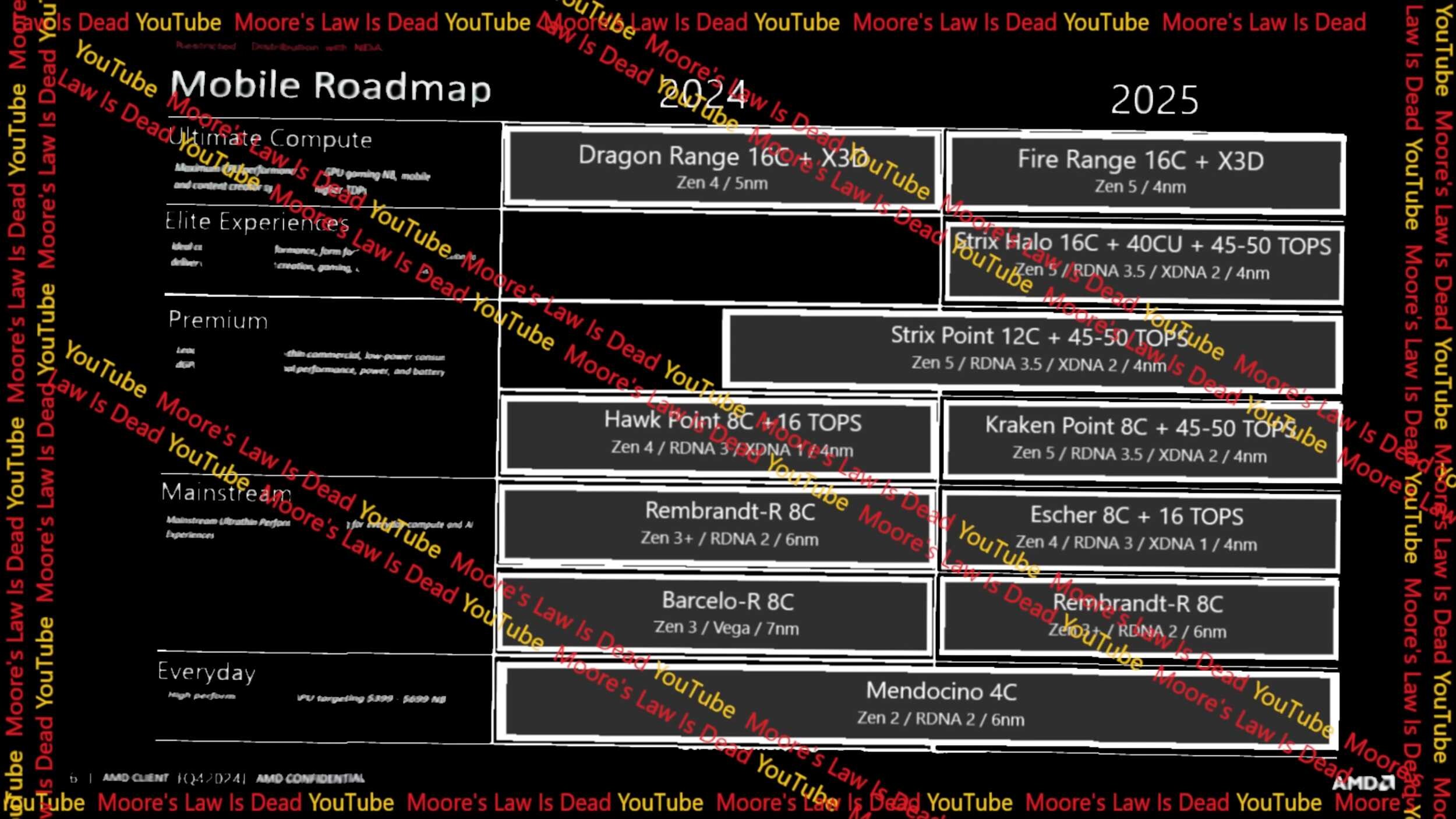
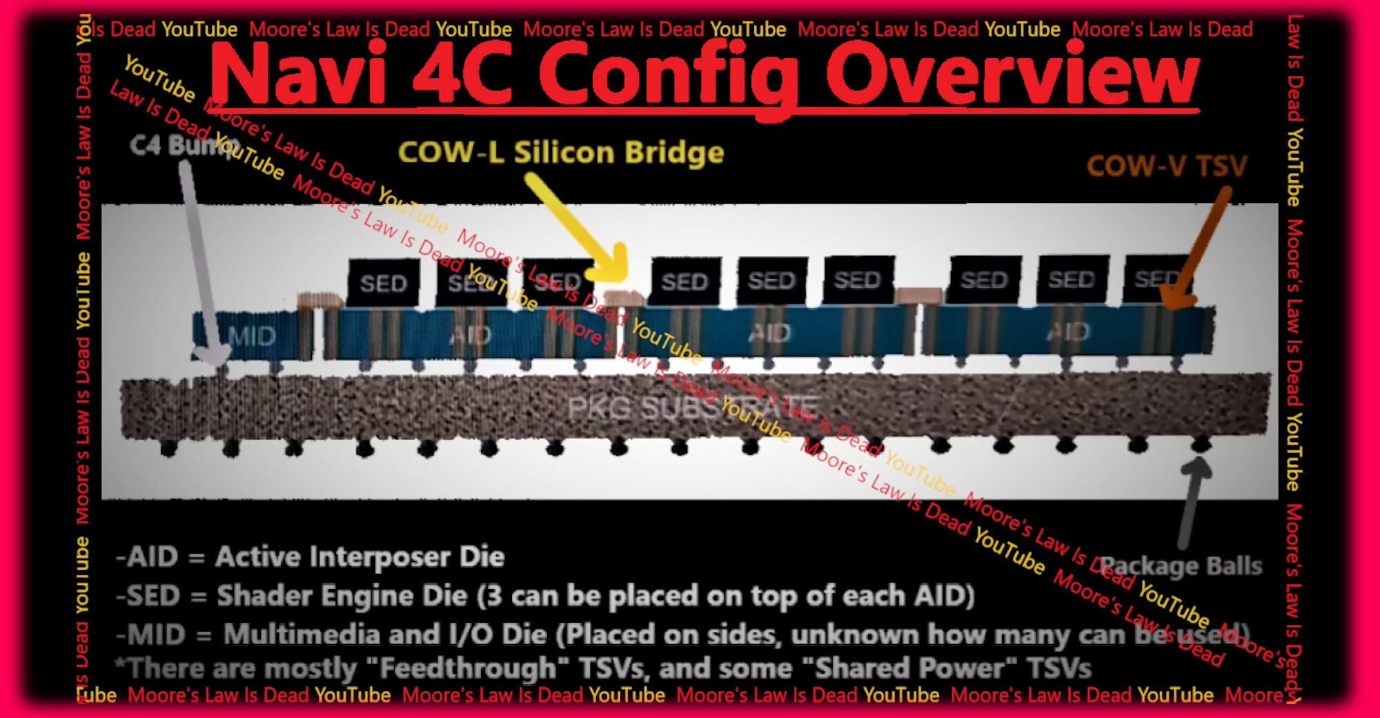
AMD Mobile Processor Lineup in 2025 Sees "Fire Range," "Strix Halo," and Signficant AI Performance Increases

With Windows 11 23H2 setting the stage for increased prevalence of AI in client PC use cases, the new hardware battleground between AMD and its rivals Intel, Apple, and Qualcomm, will be in equipping their mobile processors with sufficient AI acceleration performance. AMD already introduced accelerated AI with the current "Phoenix" processor that debuts Ryzen AI, and its Xilinx XDNA hardware backend that provides a performance of up to 16 TOPS. This will see a 2-3 fold increase with the company's 2024-25 mobile processor lineup, according to a roadmap leak by "Moore's Law is Dead."

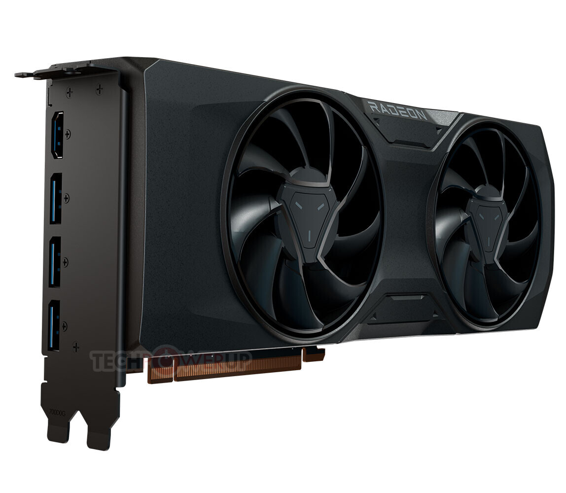
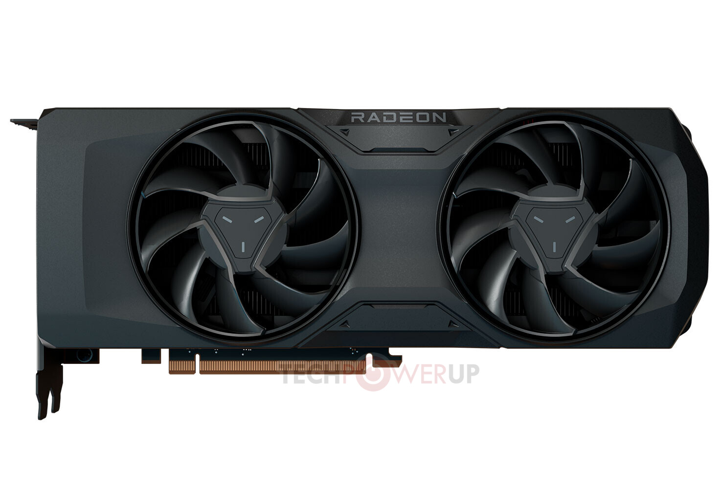
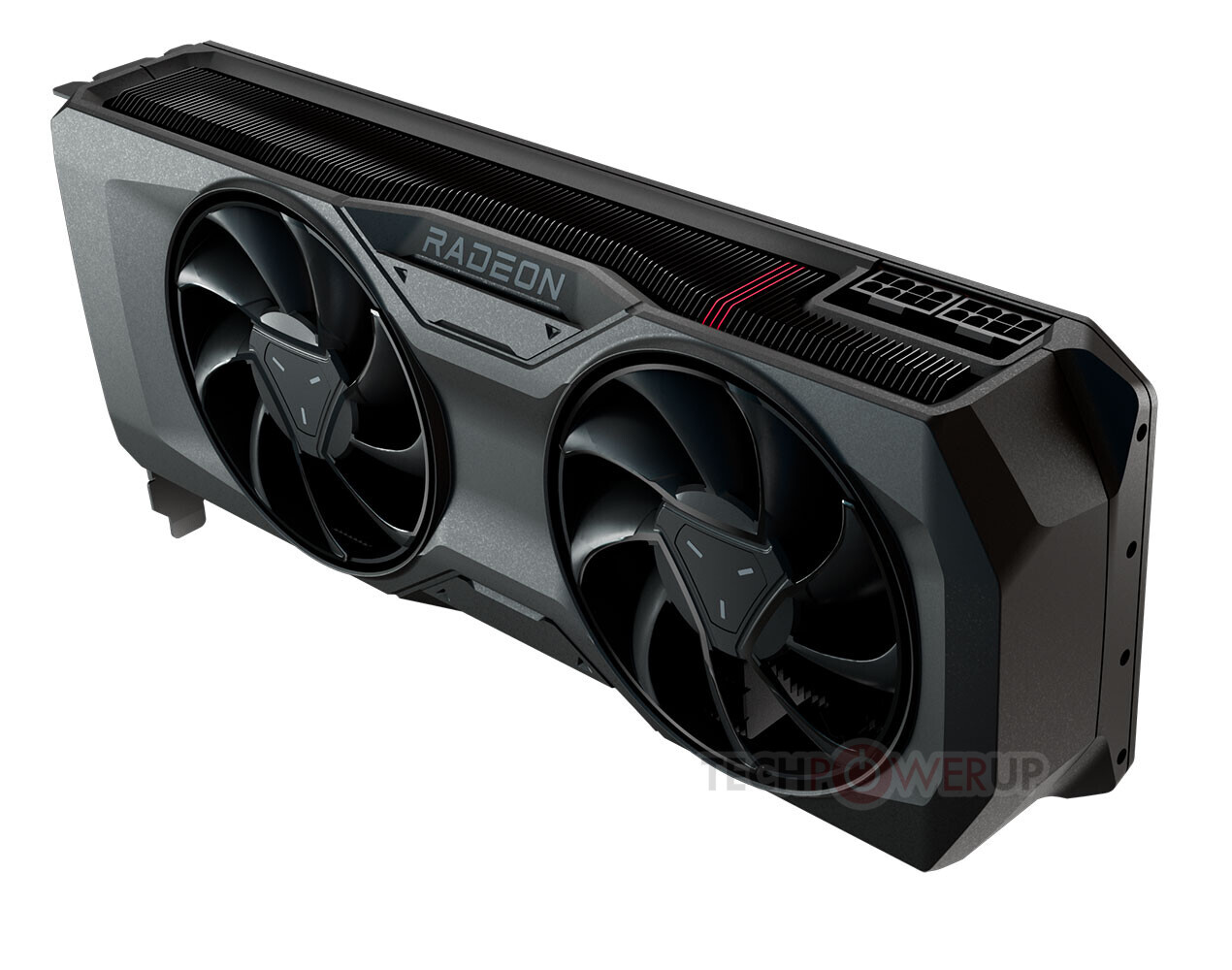
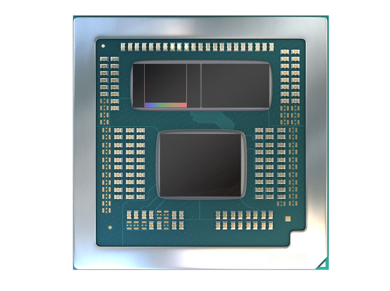
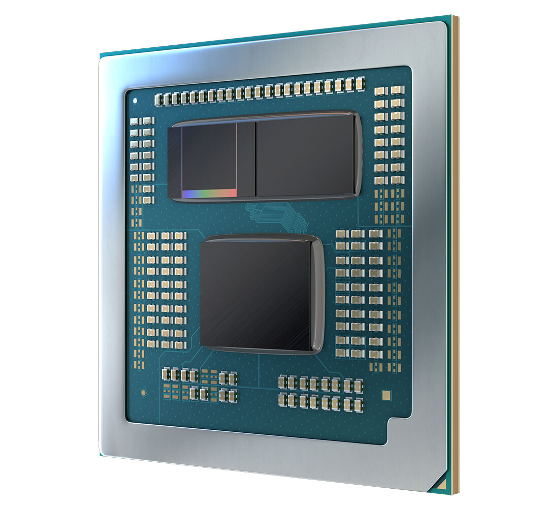
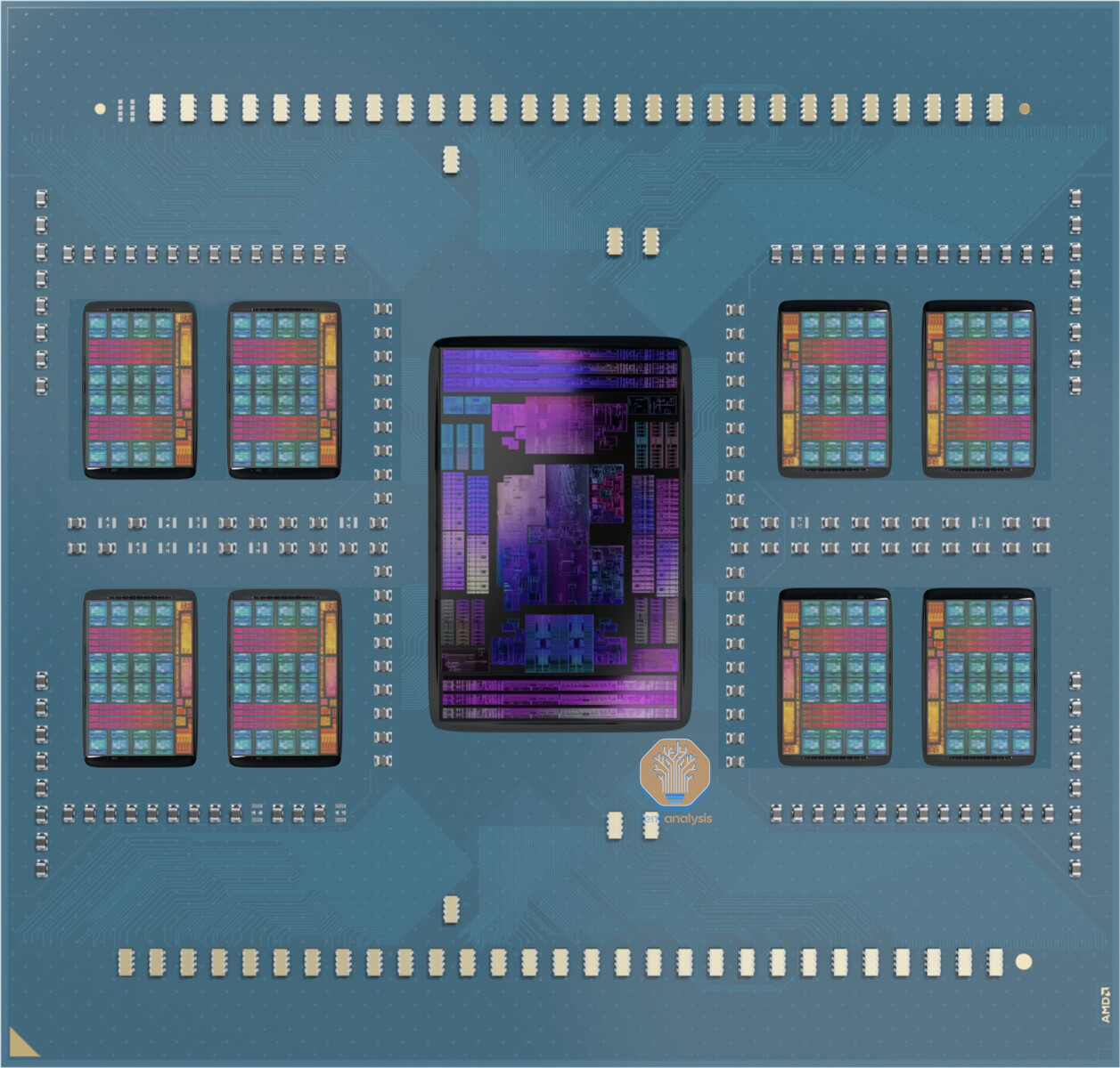
At the very top of the pile, in a product segment called "ultimate compute," which consists of large gaming notebooks, mobile workstations, and desktop-replacements; the company's current Ryzen 7045 "Dragon Range" processor will continue throughout 2024. Essentially a non-socketed version of the desktop "Raphael" MCM, "Dragon Range" features up to two 5 nm "Zen 4" CCDs for up to 16 cores, and a 6 nm cIOD. This processor lacks any form of AI acceleration. In 2025, the processor will be succeeded with "Fire Range," a similar non-socketed, mobile-friendly MCM that's derived from "Granite Ridge," with up to two 4 nm "Zen 5" CCDs for up to 16 cores; and the 6 nm cIOD. What's interesting to note here, is that the quasi-roadmap makes no mention of AI acceleration for "Fire Range," which means "Granite Ridge" could miss out on Ryzen AI acceleration from the processor. Modern discrete GPUs from both NVIDIA and AMD support AI accelerators, so this must have been AMD's consideration to exclude an XDNA-based Ryzen AI accelerator on "Fire Range" and "Granite Ridge."

US Government Can't Stop Chinese Semiconductor Advancement, Notes Former TSMC VP

The Chinese semiconductor industry is advancing, and interestingly, it is growing rapidly under sanctions, even with the blacklisting of companies by the US government. China's semiconductor industry is mainly represented by companies like Semiconductor Manufacturing International Corp (SMIC) and Huawei Technologies, who are leading the investment and progress in both chip manufacturing and chip design. According to the latest interview with Bloomberg, former TSMC Vice President Burn J. Lin said that the US government and its sanctions can not stop the advancement of Chinese semiconductor companies. Currently, Lin notes that SMIC and Huawei can use older machinery to produce more advanced chips.

Even so, SMIC could progress to 5 nm technology using existing equipment, particularly with scanners and other machinery from ASML. Development under sanctions would also force China to experiment with new materials and other chip packaging techniques that yield higher performance targets. SMIC has already developed a 7 nm semiconductor manufacturing node, which Huawei used for its latest Mate 60 Pro smartphone, based on Huawei's custom HiSilicon Kirin 9000S chip. Similarly, the transition is expected to happen to the 5 nm node as well, and it is only a matter of time before we see other nodes appear. "It is just not possible for the US to completely prevent China from improving its chip technology," noted Burn J. Lin.

Tachyum Books Purchase Order to Build System with 25,000x ChatGPT4 Capacity and 25x Faster than Current Supercomputers

Tachyum announced that it has accepted a major purchase order from a US company to build a large-scale system, based on its 5 nm Prodigy Universal Processor chip, which delivers more than 50 exaflops performance that will exponentially exceed the computational capabilities of the fastest inference or generative AI supercomputers available anywhere in the world today.

Prodigy, the world's first Universal Processor, is engineered to transform the capacity, efficiency and economics of datacenters through its industry-leading performance for hyperscale, high-performance computing and AI workloads. When complete, the Prodigy-powered system will deliver a 25x multiplier vs. the world's fastest conventional supercomputer built just this year, and will achieve AI capabilities 25,000x larger than models for ChatGPT4.

AMD EPYC 8004 "Siena" Processors with "Zen 4c" and New SP6 Platform Announced

AMD today rolled out the new compacted Socket SP6 server platform designed for smaller servers locally deployed at the edge by organizations. With CPU core-counts of up to 64-core/128-thread, these processors are based on the "Zen 4c" microarchitecture, which comes with identical IPC and ISA to "Zen 4," but with smaller L3 cache available per core. The EPYC 8004 series targets traditional data-centers located on-site for organizations. Even if the heavy-lifting of the IT for them is performed by remote data-centers or cloud providers, organizations still need smaller edge server deployments. The EPYC 8004 series caters to a different kind of servers than the ones the lower core-count models of EPYC 9004 "Genoa" do.

With the EPYC 8004 series, AMD is debuting a new smaller CPU socket called SP6. The socket measures 58.5 mm x 75.4 mm, compared to the 76.0 mm x 80.0 mm of Socket SP5 powering EPYC 9004 "Genoa" and EPYC 97x4 "Bergamo." Socket SP5 is an LGA with a pin count of 4,844, compared to SP5, which is LGA-6096. The first line of processors for this socket, the EPYC 8004 series, are codenamed "Siena." These are very much part of the 4th Gen EPYC series, a lineage it shares with "Genoa" for data-center servers, "Genoa-X" for compute servers, and "Bergamo" for high-density cloud.

Intel Foundry Services and Tower Semiconductor Announce New US Foundry Agreement

Intel Foundry Services (IFS) and Tower Semiconductor, a leading foundry for analog semiconductor solutions, today announced an agreement where Intel will provide foundry services and 300 mm manufacturing capacity to help Tower serve its customers globally. Under the agreement, Tower will utilize Intel's advanced manufacturing facility in New Mexico. Tower will invest up to $300 million to acquire and own equipment and other fixed assets to be installed in the New Mexico facility, providing a new capacity corridor of over 600,000 photo layers per month for Tower's future growth, enabling capacity to support forecasted customer demand for 300 mm advanced analog processing.

This agreement demonstrates the commitment from both Intel and Tower to expand their respective foundry footprints with unparalleled solutions and scaled capabilities. Intel will manufacture Tower's highly differentiated 65-nanometer power management BCD (bipolar-CMOS-DMOS) flows, among other flows at Intel's Fab 11X in Rio Rancho, New Mexico.

Top Ten Semiconductor Foundries Report a 1.1% Quarterly Revenue Decline in 2Q23, Anticipated to Rebound in 3Q23

TrendForce reports an interesting shift in the electronics landscape: dwindling inventories for TV components, along with a surging mobile repair market that's been driving TDDI demand, have sparked a smattering of urgent orders in the Q2 supply chain. These last-minute orders have served as pivotal lifelines, propping up Q2 capacity utilization and revenue for semiconductor foundries. However, the adrenaline rush from these stop-gap orders may be a short-lived phenomenon and is unlikely to be carried over into the third quarter.

On the other hand, demand for staple consumer products like smartphones, PCs, and notebooks remains sluggish, perpetuating a slump in the use of expensive, cutting-edge manufacturing processes. At the same time, traditionally stable sectors—automotive, industrial control, and servers—are undergoing inventory correction. The confluence of these trends has resulted in a sustained contraction for the world's top ten semiconductor foundries. Their global revenue declined by approximately 1.1% for the quarter, amounting to a staggering US$26.2 billion.

AMD Unveils Radeon RX 7800 XT and RX 7700 XT Graphics Cards

AMD today at Gamescom unveiled the Radeon RX 7800 XT and Radeon RX 7700 XT performance-segment graphics cards. Designed for maxed out gaming at 1440p with ray tracing, the two are designed to square off against NVIDIA's GeForce RTX 4070 series, offering competitive performance and pricing. The two are based on AMD's latest RDNA3 graphics architecture, and use the 5 nm foundry process where it matters. Both cards claim to offer not just superior performance to the specific NVIDIA RTX 40-series SKUs they're designed to compete with, but also better future-proofing, with more video memory on offer.

At the heart of the two is the new "Navi 32" GPU, AMD's second largest chip from this generation. It is a chiplet GPU, just like the "Navi 31" that powers the RX 7900 series, albeit slightly scaled down. The graphics compute die (GCD), the die with the main graphics rendering and compute machinery, is built on the 5 nm EUV foundry node. It is flanked by four memory cache dies (MCDs), each built on the 6 nm foundry node. These are the same MCDs found in the "Navi 31," but four in number instead of six, which gives the "Navi 32" a 256-bit wide GDDR6 memory interface.

AMD "Navi 4C" GPU Detailed: Shader Engines are their own Chiplets

"Navi 4C" is a future high-end GPU from AMD that will likely not see the light of day, as the company is pivoting away from the high-end GPU segment with its next RDNA4 generation. For AMD to continue investing in the development of this GPU, the gaming graphics card segment should have posted better sales, especially in the high-end, which it didn't. Moore's Law is Dead scored details of what could have been a fascinating technological endeavor for AMD, in building a highly disaggregated GPU.

AMD's current "Navi 31" GPU sees a disaggregation of the main logic components of the GPU that benefit from the latest 5 nm foundry node to be located in a central Graphics Compute Die; surrounded by up to six little chiplets built on the older 6 nm foundry node, which contain segments of the GPU's Infinity Cache memory, and its memory interface—hence the name memory cache die. With "Navi 4C," AMD had intended to further disaggregate the GPU, identifying even more components on the GCD that can be spun out into chiplets; as well as breaking up the shader engines themselves into smaller self-contained chiplets (smaller dies == greater yields and lower foundry costs).

AMD Radeon RX 7700 XT Confirmed with 192-bit Memory Bus in ASRock Regulatory Leak

AMD Radeon RX 7700 XT is confirmed to feature 12 GB as its standard memory size, and feature a 192-bit wide GDDR6 memory interface, according to a leaked regulatory filing by ASRock for its upcoming graphics cards. We already know from last week's mega leak of the PowerColor RX 7800 XT Red Devil that the card maxes out the "Navi 32" silicon, enabling all 60 RDNA3 CU, and comes with 16 GB of memory across the chip's full 256-bit memory bus. This filing suggests how AMD will carve the RX 7700 XT out.

Probably designed to compete with the GeForce RTX 4070, the RX 7700 XT is based on the same "Navi 32" silicon as the RX 7800 XT, but cut down. AMD is expected to disable some of the 60 CU physically present on the 5 nm GCD, while one of the four 6 nm MCDs will be disabled, giving the chip a 192-bit memory bus to drive its 12 GB of memory. We know from the PowerColor leak that the RX 7800 XT gets 18 Gbps memory speed. It remains to be seen if AMD sticks with this speed for even the RX 7700 XT, in which case, it gets 432 GB/s of memory bandwidth at its disposal. AMD is expected to launch the RX 7800 XT and RX 7700 XT within this quarter (before October).

PowerColor AMD Radeon RX 7800 XT Pictured, Confirmed Based on "Navi 32"

PowerColor inadvertently released the first pictures of its AMD Radeon RX 7800 XT Red Devil graphics card. These pictures confirm that the RX 7800 XT is based on a maxed out version of the "Navi 32" GPU, and not the compact "Navi 31" powering the limited edition RX 7900 GRE. The "Navi 32" is a chiplet-based GPU, just like the "Navi 31," albeit smaller. Its 5 nm GCD (graphics compute die) physically features 60 RDNA3 compute units, which work out to 3,840 stream processors, 120 AI accelerators, 60 Ray accelerators, 192 TMUs, and possibly 128 ROPs. This GCD is surrounded by four 6 nm MCDs (memory cache dies), which each has a 16 MB segment of the GPU's 64 MB Infinity Cache memory, and make up its 256-bit GDDR6 memory interface.

The specs sheet put out by PowerColor confirms that the RX 7800 XT maxes out the "Navi 32," enabling all 60 CUs, and the chip's full 256-bit memory interface, to drive 16 GB of memory. The RX 7800 XT uses 18 Gbps memory speed, and hence has 576 GB/s of memory bandwidth at its disposal. The PowerColor RX 7800 XT Red Devil has dual-BIOS, and assuming the "standard/silent" BIOS runs the card at AMD reference clock speeds, we're looking at Game clocks of 2210 MHz, and 2565 MHz boost. The Red Devil draws power from a dual 8-pin PCIe power connector set up (375 W max); the cooler is visibly smaller than the one on the company's RX 7900 series Red Devil cards. A 16+2 phase VRM powers the card. With pictures of the card out, we expect a global product launch within the next 30 days.

AMD Radeon RX 7900 GRE ASIC Smaller than Navi 31, Slightly Larger than Navi 21

The GPU at the heart of the China-exclusive AMD Radeon RX 7900 GRE (Golden Rabbit Edition) sparked much curiosity. It is a physically different GPU from the one found in desktop Radeon RX 7900 XT and RX 7900 XTX graphics cards. AMD wouldn't go through all that effort designing a whole different GPU just for a limited edition graphics card, which means this silicon could find greater use for the company—for example, this could be the package AMD uses for its upcoming mobile RX 7900 series. AMD wouldn't go through all the effort designing a first-party MBA (made by AMD) PCB for the silicon just for the RX 7900 GRE, and so this PCB, with this particular version of the "Navi 31" silicon, could see a wider global launch, probably as the rumored Radeon RX 7800 XT, or something else (although with a different set of specs from the RX 7900 GRE).

We compared the sizes of the new "Navi 31" package found in the RX 7900 GRE, with those of the regular "Navi 31" powering the RX 7900 XT/XTX, the previous-generation "Navi 21" powering the RX 6900 XT, and the NVIDIA AD103 silicon powering the desktop GeForce RTX 4080. There are some interesting findings. The new smaller "Navi 31" package is visibly smaller than the one powering the RX 7900 XT/XTX. It is a square package, compared to the larger rectangular one, and has a significantly thinner metal reinforcement brace. What's interesting is that the 5 nm GCD is still surrounded by six 6 nm MCDs. We don't know if they've disabled two of the six MCDs, or whether they're dummies. AMD uses dummy chiplets as structural reinforcement in some of its EPYC server processors. The dummies spread some of the mounting pressure applied by the IHS or cooling solution, so the logic behind surrounding the GCD with six of these MCDs could be the same.

AMD Announces Ryzen 9 7945X3D Flagship Mobile Processor with 3DV Cache

AMD today announced the Ryzen 9 7945X3D mobile processor, which it claims is the fastest notebook processor for gaming, faster than even Intel's Core i9-13980HX. The 7945X3D is a 16-core/32-thread processor that leverages AMD 3D Vertical Cache technology. Much like the desktop Ryzen 9 7950X3D, the 7945X3D features 64 MB of stacked 3D vertical cache memory on one of its two "Zen 4" CCDs, which gives it 96 MB of last-level cache. The second one is a regular "Zen 4" CCD with 32 MB of L3 cache—again, just like the desktop 7950X3D. The most interesting aspect has to be that AMD claims to have pulled off leadership gaming performance at a 55 W+ TDP.

The Ryzen 9 7945X3D is based on the "Dragon Range" multi-chip module. This is essentially a mobile-optimized BGA variant of the desktop "Raphael" MCM, with a higher degree of power optimization. The processor features 16 "Zen 4" CPU cores spread across two CCDs, each with 1 MB of L2 cache. The first CCD has 96 MB of L3 cache thanks to the 3DV cache, while the second CCD has 32 MB of it. Despite its power constrained form-factor, the 7945X3D has a maximum boost frequency of 5.40 GHz. Each of the two CCDs is built on the 5 nm EUV foundry node. The L3D (the die stacked on top of the first CCD) is built on 6 nm, as is the client I/O die (cIOD). The processor supports dual-channel DDR5, and has a 28-lane PCI-Express Gen 5 root complex. AMD claims that the Ryzen 9 7945X3D is on average 15% faster at gaming than its current flagship processor, the 16-core Ryzen 9 7945HX. This should mean that the processor is faster than the Intel Core i9-13980HX. The first notebook to debut the AMD Ryzen 9 7945X3D is the ASUS ROG Strix SCAR 17 X3D, which goes on sale on August 22, 2023.

Leaker Claims No Liquid Metal Cooling for PlayStation 5 Refresh

PlayStation 5-related rumors have been flowing over the past week—Zuby_Tech was reportedly the main source responsible for leaking out Project Q footage, but the tipster has turned to his attention to an alleged new version of the host system. Yesterday's tweet makes reference to a refreshed PlayStation 5 model—the "CFI-1300 series"—with a revised 5 nm APU. The late-2020 launch model (CFI-1200) sported a 7 nm chipset, while 2022's die shrink granted the CFI-1202 series with a 6 nm SoC.

The tipster thinks that Sony will be dropping the PS5's liquid metal cooling system for its next iteration, thanks to a central 5 nm part offering greater efficiency and reduced thermal output. Previous reports have predicted that this refreshed "modular model" is marked for a late 2023 release window. Sony has been running a summer price reduction campaign—could this marketing incentive be clearing the way—i.e selling off older stock—in anticipation of the refreshed model's arrival? "CFI-1300" should not be confused with the heavily rumored PlayStation 5 Pro variant—Insider Gaming's Tom Henderson has reiterated multiple times that this major hardware upgrade is still a long way off from launching.

Samsung Reveals its New Wearable Processor - Exynos W930

Make health and fitness journeys smoother with the Exynos W930—the wearable processor that keeps smartwatches ahead of the curve, with new leaps in performance and power saving.

Watch it work wonders
Exynos W930 is equipped with the Arm Cortex-A55 dual-core CPU, boosting CPU speed to 1.4 GHz for an 18% jump over our last generation processor. In-package DRAM expands to 2 GB in the Exynos W930, passing the last generation by 33%, so you can switch between apps up to 25% faster and manage your workouts and your work life better with a suite of apps performing at their best.

Radeon RX 7900 GRE Confirmed to Debut New Navi 3X GPU

It turns out that the upcoming Radeon RX 7900 GRE (Golden Rabbit Edition) is built on the mysterious Navi 31 + Navi 32 hybrid GPU that's been in the news for a few weeks now. AMD has reportedly developed its answer to NVIDIA's AD103 silicon in the form of a new MCM that combines the 5 nm GCD of the "Navi 31," along with the substrate of the "Navi 32," which is physically smaller, and only has four 6 nm MCDs. This hybrid MCM could power AMD's mobile Radeon RX 7900 series. The chip physically only has a 256-bit wide GDDR6 memory interface. AMD felt the need for such a contraption as the "Navi 31" is likely too big for mobile platforms, and because the "Navi 32" GCD with its 60 CU (3,840 stream processors) might prove inadequate against a maxed out AD104 or cut-down AD103.

VideoCardz caught whiff of the new GPU by comparing the back sides of the Sapphire RX 7900 GRE from yesterday's leak, with that of the production Sapphire RX 7900 XT/XTX NITRO+. There are visible differences in the layout of the SMDs, and the reinforcement brace behind the GPU has a square cutout, compared to the rectangular one behind the "Navi 31" powering the RX 7900 XT/XTX NITRO+. On the RX 7900 GRE, the GCD is configured with 84 CU, or the same core-config as the RX 7900 XT, albeit with the narrower 256-bit memory interface, and 64 MB of Infinity Cache memory. It's highly likely that AMD uses this GPU to carve out the Radeon RX 7800 XT (with fewer than 84 but higher than 60 CU); while creating the RX 7800 with a maxed out "Navi 32," and the RX 7700 series with a cut-down "Navi 32" (including by narrowing the memory bus width to 192-bit by disabling one of the four MCDs). AMD is reportedly planning to launch the RX 7900 GRE in China, on July 28, 2023.

Samsung's 3 nm GAA Process Identified in a Crypto-mining ASIC Designed by China Startup MicroBT

Semiconductor industry research firm TechInsights said it has found that Samsung's 3 nm GAA (gate-all-around) process has been incorporated into the crypto miner ASIC (Whatsminer M56S++) from a Chinese manufacturer, MicroBT. In a Disruptive Technology Event Brief exclusively provided to DIGITIMES Asia, TechInsights points out that the significance of this development lies in the commercial utilization of GAA technology, which facilitates the scaling of transistors to 2 nm and beyond. "This development is crucial because it has the potential to enhance performance, improve energy efficiency, keep up with Moore's Law, and enable advanced applications," said TechInsights, identifying the MicroBT ASIC chip the first commercialized product using GAA technology in the industry.

But this would also reveal that Samsung is the foundry for MicroBT, using the 3 nm GAA process. DIGITIMES Research semiconductor analyst Eric Chen pointed out that Samsung indeed has started producing chips using the 3 nm GAA process, but the capacity is still small. "Getting revenues from shipment can be defined as 'commercialization', but ASIC is a relatively simple kind of chip to produce, in terms of architecture."

DEEPX Announces State-of-the-Art AI Chip Product Lineup

DEEPX, a leading AI semiconductor technology company, aims to drive innovation in the rapidly evolving edge AI landscape with its state-of-the-art, low-power, high-performance AI chip product lineup. With a focus on revolutionizing application areas such as smart cities, surveillance, smart factories, and other industries, DEEPX unveiled its latest AI semiconductor solutions at the 2023 Samsung Foundry Forum (SFF), under the theme of "For AI Everywhere."

Recognizing the importance of collaboration and technological partnerships, DEEPX leveraged Samsung Electronics' foundry processes, harnessing the power of 5 nm, 14 nm, and 28 nm technologies for its semiconductor chip designs. As a result, the company has developed a suite of four high-performance, energy-efficient AI semiconductor products: DX-L1, DX-L2, DX-M1, and DX-H1. Each product has been specifically engineered to cater to the unique demands of various market segments, from ultra-compact sensors with minimal data processing requirements to AI-intensive applications such as robotics, computer vision, autonomous vehicles, and many others.

AMD Planning September Launch for Radeon RX 7800 series and RX 7700 series

AMD is planning to plug the Atlantic gap between its mainstream Radeon RX 7600 and enthusiast-class RX 7900 XT with the RX 7800 series and RX 7700 series, with either an announcement or teaser planned for 2023 Gamescom, which is scheduled for August. There could be up to four new graphics card SKUs announced, with their product launches spread across Q3 and Q4 2023. The "Navi 32" MCM is expected to power at least three of these SKUs, while it was recently rumored that AMD could design a new GPU that has the GCD of the "Navi 31" on the package of "Navi 32" with its four MCDs, to end up with a higher CU count than what the "Navi 32" can offer.

The "Navi 32" GPU is an MCM, just like the "Navi 31" powering the RX 7900 series. It is rumored to feature a 5 nm GCD (graphics compute die) with 60 RDNA3 compute units, which work out to 3,840 stream processors, 120 AI accelerators, 60 Ray Accelerators, 240 TMUs, and possibly 128 ROPs. The four 6 nm MCDs give it 64 MB of Infinity Cache, and a 256-bit wide GDDR6 memory interface. Assuming the RX 7800 XT uses the unnamed new MCM with the GCD of the "Navi 31" that has a CU count somewhere between 60 and 72, a maxed-out "Navi 32" could power the RX 7800, while its cut-down variants power the RX 7700 XT and RX 7700.

ICYMI, GeForce RTX 4060 Launched Last Week: A Summary of our Mammoth Coverage

Last week (June 29), NVIDIA launched the GeForce RTX 4060 "Ada" graphics card targeting a majority of PC gamers who still play at 1080p Full HD resolution. Reception to the new card was somewhat lukewarm, only 6% of our polled readers are interested in buying one (poll results). We crunched thousands of benchmark runs in our new 2023H2 test suite and managed to review ten different models of the 4060, six of which are available at the NVIDIA MSRP of $299, and we followed up with four more reviews of premium custom-design cards priced above the MSRP. Our results confirm that GeForce RTX 4060 is designed for maxed out gaming at 1080p; gameplay with ray tracing is possible at 25-50 FPS at 1080p, which can be increased by dialing down graphics settings, or through use of DLSS and DLSS 3 Frame Generation, in supported games. On the other hand, there were concerns with the small performance gains and high pricing, which makes many other options a viable choice.

We've put together a video presentation which compares all the cards tested, and that also serves as a really quick executive summary of the RTX 4060, and whether you should get one.

Samsung Electronics Unveils Foundry Vision in the AI Era

Samsung Electronics, a world leader in advanced semiconductor technology, today announced its latest foundry technology innovations and business strategy at the 7th annual Samsung Foundry Forum (SFF) 2023. Under the theme "Innovation Beyond Boundaries," this year's forum delved into Samsung Foundry's mission to address customer needs in the artificial intelligence (AI) era through advanced semiconductor technology.

Over 700 guests, from customers and partners of Samsung Foundry, attended this year's event, of which 38 companies hosted their own booths to share the latest technology trends in the foundry industry.

Radeon RX 7800 XT Based on New ASIC with Navi 31 GCD on Navi 32 Package?

AMD Radeon RX 7800 XT will be a much-needed performance-segment addition to the company's Radeon RX 7000-series, which has a massive performance gap between the enthusiast-class RX 7900 series, and the mainstream RX 7600. A report by "Moore's Law is Dead" makes a sensational claim that it is based on a whole new ASIC that's neither the "Navi 31" powering the RX 7900 series, nor the "Navi 32" designed for lower performance tiers, but something in between. This GPU will be AMD's answer to the "AD103." Apparently, the GPU features the same exact 350 mm² graphics compute die (GCD) as the "Navi 31," but on a smaller package resembling that of the "Navi 32." This large GCD is surrounded by four MCDs (memory cache dies), which amount to a 256-bit wide GDDR6 memory interface, and 64 MB of 2nd Gen Infinity Cache memory.

The GCD physically features 96 RDNA3 compute units, but AMD's product managers now have the ability to give the RX 7800 XT a much higher CU count than that of the "Navi 32," while being lower than that of the RX 7900 XT (which is configured with 84). It's rumored that the smaller "Navi 32" GCD tops out at 60 CU (3,840 stream processors), so the new ASIC will enable the RX 7800 XT to have a CU count anywhere between 60 to 84. The resulting RX 7800 XT could have an ASIC with a lower manufacturing cost than that of a theoretical Navi 31 with two disabled MCDs (>60 mm² of wasted 6 nm dies), and even if it ends up performing within 10% of the RX 7900 XT (and matching the GeForce RTX 4070 Ti in the process), it would do so with better pricing headroom. The same ASIC could even power mobile RX 7900 series, where the smaller package and narrower memory bus will conserve precious PCB footprint.

AMD Also Launches the Ryzen PRO 7000 AM5 Processors for Commercial Desktops

In addition to the Ryzen PRO 7045 series mobile processors for commercial notebooks, AMD announced the Ryzen PRO 7000 processors for commercial desktops. These are desktops deployed by medium-large businesses and enterprises in their offices, which remain connected to the enterprise network at all times, and require remote management and security features. This particular segment is addressed by Intel using its 13th Gen Core vPro processors. The Ryzen PRO 7000 processors are based on the Socket AM5 platform, which is ready for next-generation connectivity. AMD is also introducing a new motherboard chipset to go with these processors, although they are compatible with consumer AMD 600-series chipset motherboards.

The Ryzen PRO 7000 series processor models being launched today are based on the "Raphael" MCM, which depending on the model, comes with one or two 5 nm "Zen 4" CCDs, and a 6 nm I/O die. What makes these processors especially formidable compared to past attempts by AMD at commercial desktop processors, is that while the previous-generation chips were based on monolithic APU dies for their integrated graphics; these chips are based on the full-featured MCM for this generation, with integrated graphics as standard. AMD's decision to make integrated graphics standard should prove particularly helpful for adoption in the commercial desktop space.

AMD EPYC "Bergamo" Uses 16-core Zen 4c CCDs, Barely 10% Larger than Regular Zen 4 CCDs

A SemiAnalysis report sheds light on just how much smaller the "Zen 4c" CPU core is compared to the regular "Zen 4." AMD's upcoming high core-count enterprise processor for cloud data-center deployments, the EPYC "Bergamo," is based on the new "Zen 4c" microarchitecture. Although with the same ISA as "Zen 4," the "Zen 4c" is essentially a low-power, lite version of the core, with significantly higher performance/Watt. The core is physically smaller than a regular "Zen 4" core, which allows AMD to create CCDs (CPU core dies) with 16 cores, compared to the current "Zen 4" CCD with 8.

The 16-core "Zen 4c" CCD is built on the same 5 nm EUV foundry node as the 8-core "Zen 4" CCD, and internally features two CCX (CPU core complex), each with 8 "Zen 4c" cores. Each of the two CCX shares a 16 MB L3 cache among the cores. The SemiAnalysis report states that the dedicated L2 cache size of the "Zen 4c" core remains at 1 MB, just like that of the regular "Zen 4." Perhaps the biggest finding is their die-size estimation, which puts the 16-core "Zen 4c" CCD just 9.6% larger in die-area, than the 8-core "Zen 4" CCD. That's 72.7 mm² per CCD, compared to 66.3 mm² of the regular 8-core "Zen 4" CCD.

India Homegrown HPC Processor Arrives to Power Nation's Exascale Supercomputer

With more countries creating initiatives to develop homegrown processors capable of powering powerful supercomputing facilities, India has just presented its development milestone with Aum HPC. Thanks to information from the report by The Next Platform, we learn that India has developed a processor for powering its exascale high-performance computing (HPC) system. Called Aum HPC, the CPU was developed by the National Supercomputing Mission of the Indian government, which funded the Indian Institute of Science, the Department of Science and Technology, the Ministry of Electronics and Information Technology, and C-DAC to design and manufacture the Aum HPC processors and create strong, strong technology independence.

The Aum HPC is based on Armv8.4 CPU ISA and represents a chiplet processor. Each compute chiplet features 48 Arm Zeus Cores based on Neoverse V1 IP, so with two chiplets, the processor has 96 cores in total. Each core gets 1 MB of level two cache and 1 MB of system cache, for 96 MB L2 cache and 96 MB system cache in total. For memory, the processor uses 16-channel 32-bit DDR5-5200 with a bandwidth of 332.8 GB/s. To expand on that, HBM memory is present, and there is 64 GB of HBM3 with four controllers capable of achieving a bandwidth of 2.87 TB/s. As far as connectivity, the Aum HPC processor has 64 PCIe Gen 5 Lanes with CXL enabled. It is manufactured on a 5 nm node from TSMC. With a 3.0 GHz typical and 3.5+ GHz turbo frequency, the Aum HPC processor is rated for a TDP of 300 Watts. It is capable of producing 4.6+ TeraFLOPS per socket. Below are illustrations and tables comparing Aum HPC to Fujitsy A64FX, another Arm HPC-focused design.

NVIDIA RTX 4060 Ti 16GB Model Features 5W Higher TDP, Slightly Different ASIC Code

NVIDIA is launching 8 GB and 16 GB variants of its upcoming GeForce RTX 4060 Ti graphics card, with the 8 GB model debuting later this month, and the 16 GB model slated for July, as we learned in an older article. We are learning what else sets the two apart. Both are based on the 5 nm "AD106" silicon, by enabling 34 out of 36 SM physically present on the silicon, which works out to 4,352 out of 4,608 CUDA cores present. While the 8 GB model has the ASIC code "AD106-350," the 16 GB model gets the ASIC code "AD106-351."

The 16 GB model of the RTX 4060 Ti also has a slightly higher TDP, rated at 165 W, compared to 160 W of the 8 GB model. This is the TDP of the silicon, and not TGP (typical graphics power,) which takes into account power drawn by the entire board. The 16 GB model is sure to have a higher TGP on account of its higher-density memory. NVIDIA is likely to use four 32 Gbit (4 GB) GDDR6 memory chips to achieve 16 GB (as opposed to eight 16 Gbit ones with two chips piggybacked per 32-bit path).
Return to Keyword Browsing
May 8th, 2024 08:13 EDT change timezone

New Forum Posts

Popular Reviews

Controversial News Posts