News Posts matching #AVX2

Return to Keyword Browsing

Intel Binary Optimization Tool Changes Code Execution with Heavy Vectorization

The Intel Binary Optimization Tool (BOT) has been launched alongside the "Arrow Lake Refresh" series of processors, which includes the Core Ultra 5 250K Plus and Core Ultra 7 270K Plus models. While the tool is beneficial for gamers looking to extract a few extra frames from their setups, it may be a nightmare for makers of benchmarking tools like Geekbench by Primate Labs. Recently, Primate Labs testing found that BOT changes the way .exe applications run and concluded that Geekbench runs will now flag these BOT-enhanced runs. However, in deeper testing, Primate Labs discovered that Intel's BOT may deliver significant boosts in some applications like Object Remover and HDR, increasing performance by up to 30%. This is thanks to the deep vectorization that the BOT performs behind the scenes to optimize performance.

For example, Primate Labs used Intel's own Software Development Emulator (SDE) to measure how many instructions were executed and which types of instructions the program executed. Without BOT, Geekbench 6 required a total of 1.26 trillion instructions to finish, while a BOT-enhanced run completed with 1.08 trillion instructions. This is an impressive 14% reduction. However, when examining the execution by type, we see that BOT makes heavy use of vector instructions like SSE2 and AVX2. The number of scalar instructions needed to execute a program fell from 220 billion to 84.6 billion, while the number of vector instructions increased from 1.25 billion to 18.3 billion, a 13.7x increase. This means that Intel BOT finds a way to turn inefficient scalar code into vectorized instructions that are processed much more efficiently inside Intel CPUs. These techniques indicate a very complex behind-the-scenes process than was originally believed. The Geekbench v6.7 update will include a flag for BOT, allowing future Geekbench results to be easily distinguished as BOT-enhanced or not.

Intel Publishes "Granite Rapids-WS" Xeon 600 Turbo Frequencies, AVX-512 and AMX Slash Boost Speeds

In early February, Intel finally updated its HEDT sector with the latest "Granite Rapids-WS" Xeon 600 Series processors for workstations. The company has now published a detailed table of turbo frequencies that provides specifics on each core's boost frequency in workloads like SSE, AVX2, AVX-512, and AMX, showing how much these workloads allow the CPU cores to boost. This means that during a continuous workload like AMX, these CPUs can only run at a sustained frequency defined in the tables below. At the very top of the new "Granite Rapids-WS" stack is the Xeon 698X, featuring 86 cores and 172 threads, backed by 336 MB of L3 cache. The chip runs at a 2.0 GHz base clock, boosting up to 4.8 GHz with Turbo Boost Max 3.0, or 4.6 GHz under Turbo Boost 2.0. This CPU is fully unlocked, allowing overclocking, which is still relatively rare in the Xeon workstation space.

In non-AVX workloads, this CPU can boost up to 4.8 GHz, while its lowest-performing core, numbered 86, sits at 3.0 GHz. However, AVX2 turbo frequencies cause a significant frequency downgrade, as the base frequency drops to 1.7 GHz, and the slowest core drops to 2.9 GHz when boosting across its 86-core design. Following this are the AVX-512 turbo frequencies, which see this flagship SKU running at a base clock speed of only 1.3 GHz and only 2.5 GHz across its 86 cores. Perhaps the most demanding turbo frequency testing occurs when AMX is enabled, resulting in a base frequency of only 1.1 GHz and only 2.0 GHz across all cores at once. This significant reduction comes from the demanding scenarios of these vector and matrix instruction processing, which are very heavy on the CPU.
More information about other SKUs and details in AVX2, AVX-512, and AMX turbo frequencies follow.

AMD Zen 7 to Implement AVX10 and ACE Instruction Sets

AMD on Tuesday unveiled its future "Zen 7" CPU microarchitecture. The company has been pivoting toward making its CPU IP more AI-relevant, so future processing workloads could better leverage the serial processing power of CPUs. Among these, the two important ones are AVX10 and ACE. AVX10 sees a unification of AVX-512 and AVX2 features to improve performance and compatibility across vector math heavy workloads. ACE, or Advanced Matrix Extensions for Matrix Manipulation, is an industry-standard matrix math instruction set that could prove to be relevant to every device ranging from smartphones to servers.

Among the other ISA additions with Zen 7 are FRED (flexible return and event delivery), which replaces the current device interrupt model to reduce system-level latency. Zen 7 also implements ChkTag x86 Memory Tagging to counteract several kinds of memory-level data vulnerabilities caused by buffer overflows and use-after-free errors. FRED in particular was a noteworthy feature Intel was working on for its x86S machine architecture standard.

Intel "Nova Lake" Could Arrive Without AVX10, APX, and AMX Support

Intel is still finalizing its next-generation "Nova Lake" specifications. However, the core microarchitecture has been done, the NPU design is finished and upgraded, and the instruction set is finalized. It could be the case that these consumer CPUs will again lack support for Intel's AVX10, APX, and AMX instruction set—designed to encompass 512-bit acceleration and fast vector/matrix multiplication for tasks like content creation, encoding/decoding, AI, and much more—remaining exclusive to Intel Xeon processors. According to the latest GCC compiler patch, the initial Nova Lake enablement patch does not include AVX10, AMX, or APX. This might suggest that support for these new x86 instructions could be missing from the next-generation CPU. Initially, Intel decided to disable AVX-512 for "Alder Lake" and "Raptor Lake" client-oriented CPU lineups, meaning that only server-grade Xeon CPUs got the accelerated 512-bit data paths.

This GCC patch seems to contradict the findings from August, when Intel introduced AVX10.2 support for "future Intel Core processors" in the oneDNN software library, likely targeting the Nova Lake series. We need to wait for more information from other enablement patches or direct confirmation from Intel regarding whether AVX10, APX, and AMX will be included in the 52-core Nova Lake SKUs. Enabling fast vector and matrix acceleration on 52 cores would be ideal for consumers, content creators, gamers, and workstation users alike. In comparison, AMD introduced full AVX-512 support with its "Zen 5" cores across its product range, providing a performance boost in optimized applications for both desktop and server CPUs. This marked the first time AMD did not emulate 512-bit AVX, which previously required splitting 512-bit data into two 256-bit units to be processed over two cycles.

Microsoft Readies Windows-on-Arm for Gaming With AVX/AVX2 Support

With the release of the October 2025 cumulative update (KB5066835) for Windows 11 versions 24H2 and 25H2, Microsoft has expanded Prism emulation for Arm64 devices. This update enables Windows to emulate x86 vector instructions such as AVX and AVX2 on Arm PCs. As a result, many apps and games that previously couldn't run on Arm hardware can now at least launch. Intel's AVX is a set of SIMD instructions commonly used by media tools, game engines, and creative applications to speed up tasks like video encoding, physics, and effects. Arm-based chips like Snapdragon do not natively support Intel's proprietary AVX instructions, which often led to failures or poor performance in these programs. Prism's emulation translates AVX instructions, allowing these programs to run on Arm devices. However, because it is emulation, there is additional CPU overhead, and performance will vary significantly depending on the application.

Arm, on the other hand, offers the Scalable Vector Extension (SVE), which enhances vector processing capabilities in the Armv8-A architecture, with SVE2 being its successor in Armv9-A. Unlike traditional SIMD designs with fixed-size vectors, SVE supports flexible vector lengths from 128 to 2048 bits in 128-bit increments. This flexibility allows chip manufacturers to select the vector size that best suits their processors. The main advantage is that programs written for SVE can run on any SVE-compatible processor without recompilation, regardless of the processor's vector size.

Zhaoxin KH-50000 CPU Family Brings 96 Cores, DDR5, and ZPI 5.0

Chinese company Zhaoxin has announced the KH-50000 series, its most advanced server processors to date, built around a chiplet layout that clusters 12 compute dies with a large central I/O die. The top models offer up to 96 high-performance cores per socket and are available for dual- and quad-socket configurations, enabling systems with up to 384 cores. Zhaoxin quotes a base clock ranging from 2.2/2.6 GHz with boost frequencies reaching 3.0 GHz, and the family includes a substantial shared L3 cache measured up to 384 MB. Memory support expands to 12 channels of DDR5 ECC RDIMM, with per-socket capacities designed to accommodate 3 TB. The company envisions the KH-50000 as a versatile engine for cloud, AI inference, big-data analytics, and general-purpose enterprise workloads while emphasizing domestic supply chain independence and platform compatibility with existing x86 software stacks. It also includes extended platform validation and vendor support.

I/O and system interconnects form a core part of the KH-50000 story: the platform delivers 128 lanes of PCIe 5.0 with ZPI/CXL semantics, plus 16 additional PCIe 4.0 lanes and legacy SATA and USB links. Zhaoxin shows a new ZPI 5.0 interconnect designed to enhance bandwidth and reduce latency and power consumption across multi-socket configurations, enabling servers to scale performance without incurring linear energy costs. The design retains x86 32/64-bit instruction compatibility with AVX2 support and incorporates cryptographic accelerators for regional standards, aiming to resemble modern high-density server layouts. Compared to the KH-40000 family launches in 2022, Zhaoxin triples the maximum core count, transitions from DDR4 to DDR5 memory, increases cache capacity, and upgrades platform I/O to the latest generation. The firm says partners will begin validating systems soon, and it hinted at future KX consumer and AI-oriented parts that integrate NPUs for accelerated workloads. Rollout to domestic vendors is expected later in the next few months.

Zhaoxin Launches KX-7000 Desktop 8-Core x86 Processor to Power China's Ambitions

After years of delays, Chinese chipmaker Zhaoxin has finally launched its long-awaited KX-7000 series consumer CPUs, only one of its kind in China, based on the licensed x86-64 ISA. Zhaoxin claims the new 8-core processors based on "Century Avenue" uArch deliver double the performance of previous generations. Leveraging architectural improvements and 4X more cache, the KX-7000 represents essential progress for China's domestic semiconductor industry. While still likely lagging behind rival AMD and Intel chips in raw speed, the KX-7000 matches competitive specs in areas like DDR5 memory, PCIe 4.0, and USB4 support. For Chinese efforts to attain technological independence, closing feature gaps with foreign processors is just as crucial as boosting performance. Manufactured on a 16 nm process, the KX-7000 does not use the best silicon node available.

Other chip details include out-of-order execution (OoOE), 24 PCIe 4.0 lanes, a 32 MB pool of L3 cache and 4 MB L2 cache, a base frequency of 3.2 GHz, and a boost clock of 3.7 GHz. Interestingly, the CPU also has VT-x, BT-d 2.5, SSE4.2/AVX/AVX2 support, most likely also licensed from the x86 makers Intel and/or AMD. Ultimately, surpassing Western processors is secondary for China next to attaining self-reliance. Instructions like SM encryption catering to domestic data protection priorities underscore how the KX-7000 advances strategic autonomy goals. With its x86 architecture license giving software compatibility and now a vastly upgraded platform, the KX-7000 will raise China's chip capabilities even if it is still trailing rivals' speeds. Ongoing progress closing that performance gap could position Zhaoxin as a mainstream alternative for local PC builders and buyers.

"Downfall" Intel CPU Vulnerability Can Impact Performance By 50%

Intel has recently revealed a security vulnerability named Downfall (CVE-2022-40982) that impacts multiple generations of Intel processors. The vulnerability is linked to Intel's memory optimization feature, exploiting the Gather instruction, a function that accelerates data fetching from scattered memory locations. It inadvertently exposes internal hardware registers, allowing malicious software access to data held by other programs. The flaw affects Intel mainstream and server processors ranging from the Skylake to Rocket Lake microarchitecture. The entire list of affected CPUs is here. Intel has responded by releasing updated software-level microcode to fix the flaw. However, there's concern over the performance impact of the fix, potentially affecting AVX2 and AVX-512 workloads involving the Gather instruction by up to 50%.

Phoronix tested the Downfall mitigations and reported varying performance decreases on different processors. For instance, two Xeon Platinum 8380 processors were around 6% slower in certain tests, while the Core i7-1165G7 faced performance degradation ranging from 11% to 39% in specific benchmarks. While these reductions were less than Intel's forecasted 50% overhead, they remain significant, especially in High-Performance Computing (HPC) workloads. The ramifications of Downfall are not restricted to specialized tasks like AI or HPC but may extend to more common applications such as video encoding. Though the microcode update is not mandatory and Intel provides an opt-out mechanism, users are left with a challenging decision between security and performance. Executing a Downfall attack might seem complex, but the final choice between implementing the mitigation or retaining performance will likely vary depending on individual needs and risk assessments.

AAEON UP 7000 Brings Intel Processor N-series Onboard the World's Smallest Platform

AAEON's UP brand, renowned for producing sophisticated developer boards with industrial-grade specifications, has announced the release of the UP 7000, the third generation of boards built on the 85 mm x 56 mm form factor of the original UP Board. The UP 7000 boasts numerous upgrades compared to its predecessors, including 8 GB of LPDDR5 system memory, onboard TPM 2.0, and support for both Windows and Linux OS. Most notably, it stands out as the world's smallest board featuring onboard CPUs from the Intel Processor N-series platform.

The board is available in various SKUs, hosting Intel Processor N97, Intel Processor N100, or Intel Processor N50 CPUs. Notably, these processors offer clock speeds up to 50% faster than those of previous boards from the same product line, and also support Intel AVX2 for energy-efficient AI acceleration. Equipped with three USB Type-A ports for USB 3.2 Gen 2, one GbE LAN port supporting Realtek RTL8111H CG, and a Raspberry Pi-compatible 40-pin HAT for expansion, the UP 7000 provides a dense port configuration. This makes it ideal for applications requiring low latency but versatile connectivity, such as AMR and multifunction printing device solutions.

Intel Publishes Sorting Library Powered by AVX-512, Offers 10-17x Speed Up

Intel has recently updated its open-source C++ header file library for high-performance SIMD-based sorting to support the AVX-512 SIMD instruction set. Extending the capability of regular AVX2 support, the sorting functions now implement 512-bit extensions to offer greater performance. According to Phoronix, the NumPy Python library for mathematics that underpins a lot of software has updated its software base to use the AVX-512 boosted sorting functionality that yields a fantastic uplift in performance. The library uses AVX-512 to vectorize the quicksort for 16-bit and 64-bit data types using the extended instruction set. Benchmarked on an Intel Tiger Lake system, the NumPy sorting saw a 10-17x increase in performance.

Intel's engineer Raghuveer Devulapalli changed the NumPy code, which was merged into the NumPy codebase on Wednesday. Regarding individual data types, the new implementation increases 16-bit int sorting by 17x and 32-bit data type sorting by 12-13x, while float 64-bit sorting for random arrays has experienced a 10x speed up. Using the x86-simd-sort code, this speed-up shows the power of AVX-512 and its capability to enhance the performance of various libraries. We hope to see more implementations of AVX-512, as AMD has joined the party by placing AVX-512 processing elements on Zen 4.

Intel Core i9-13900 "Raptor Lake" Processor Gets a Preview

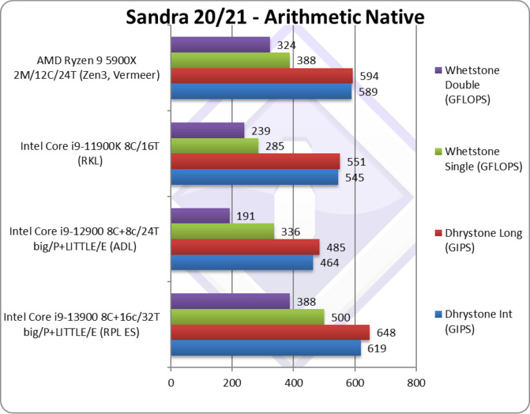
Intel is preparing to launch its 13th generation of desktop processors codenamed Raptor Lake. Succeeding Alder Lake, the 13th gen design will implement up to eight P-cores with 16 E-cores manufactured on Intel's improved 7+ technology node. Today, we got a performance preview from SiSoftware that has collected SiSoftware Sandra database scores of Intel Core i9-13900 Raptor Lake-S processor. They present an overview of a few benchmarks. Firstly, the SoC features 36 MB of unified L3 cache versus 30 MB in Alder Lake. With DDR5 memory running up to 5600 MT/s and PCIe 5.0, the SoC features the latest IO and memory standards. The big P-cores now lack AVX-512 and feature 2 MB of L2 cache per core. We see 4 MB of L2 cache for a cluster of small E-cores. An exciting addition to E-cores is the AVX/AVX2 support, which is a first for Atom cores.

Regarding testing, the author has collected a few tests that seemed appropriate to compare to the equivalent Alder Lake model. Starting with ALU/FPU tests that benchmark basic arithmetic tasks, Raptor Lake delivered 33% to 50% improvement over Alder Lake. The Raptor Lake design achieved this with 3.7 GHz P-Core and 2.76 GHz E-Core frequency. In vectorized and SIMD tests, the 13th gen design showed only 5% to 8% improvement over the previous generation. For more benchmarks and accurate results, we have to wait for TechPowerUp's test, which will be coming on the release day.

MSI Partially Reenables AVX-512 Support for Alder Lake-S Processors

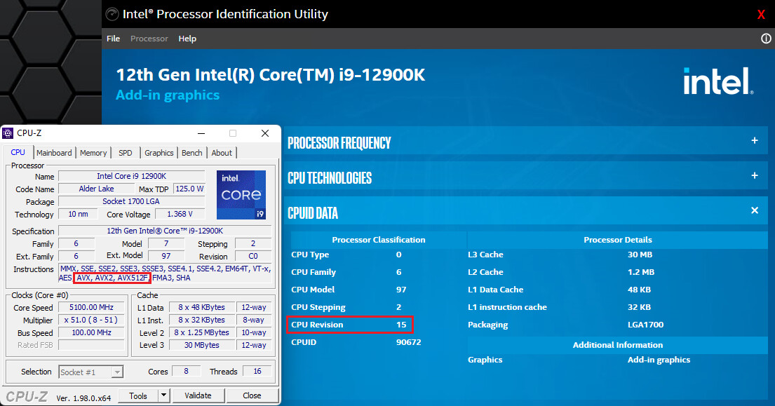
Intel's Alder Lake processors have two types of cores present, with two distinct sets of features and capabilities enabled. For example, smaller E-cores don't support the execution of AVX-512 instructions, while the bigger P-cores have support for AVX-512 instructions. So Intel has decided to remove support for it altogether not to create software errors and run into issues with executing AVX-512 code on Alder Lake processors. This happened just months before the launch of Alder Lake, making us see some initial motherboard BIOSes come with AVX-512 enabled from the box. Later on, all motherboard makers pulled the plug on it, and it is a rare sight to see support for it.

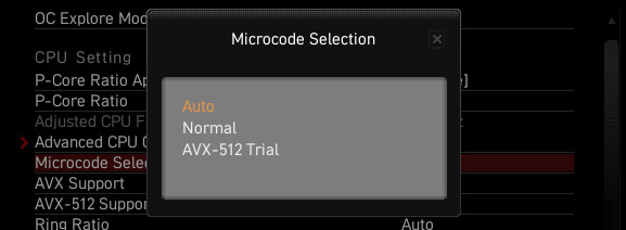
However, it seems like MSI is unhappy with the lack of AVX-512, and the company is reenabling partial support for it. According to Xaver Amberger, editor at Igor's Lab, MSI reintroduces selecting microcode version with its MEG Z690 Unify-X motherboard. There is an option for AVX-512 enablement in the menu, and it is indeed a functional one. With BIOS A22, MSI enabled AVX-512 instruction execution, and there are benchmarks to prove it works. This shows an advantage of 512-bit wide execution units of AVX-512 over something like AVX2, which offers only 256-bit wide execution units. In applications such as Y-Cruncher, AVX-512 enabled the CPU to reach higher performance targets while consuming less power.
Return to Keyword Browsing
Nov 11th, 2026 07:09 CST change timezone

New Forum Posts

Popular Reviews

TPU on YouTube

Controversial News Posts