News Posts matching #Eldora

Return to Keyword Browsing

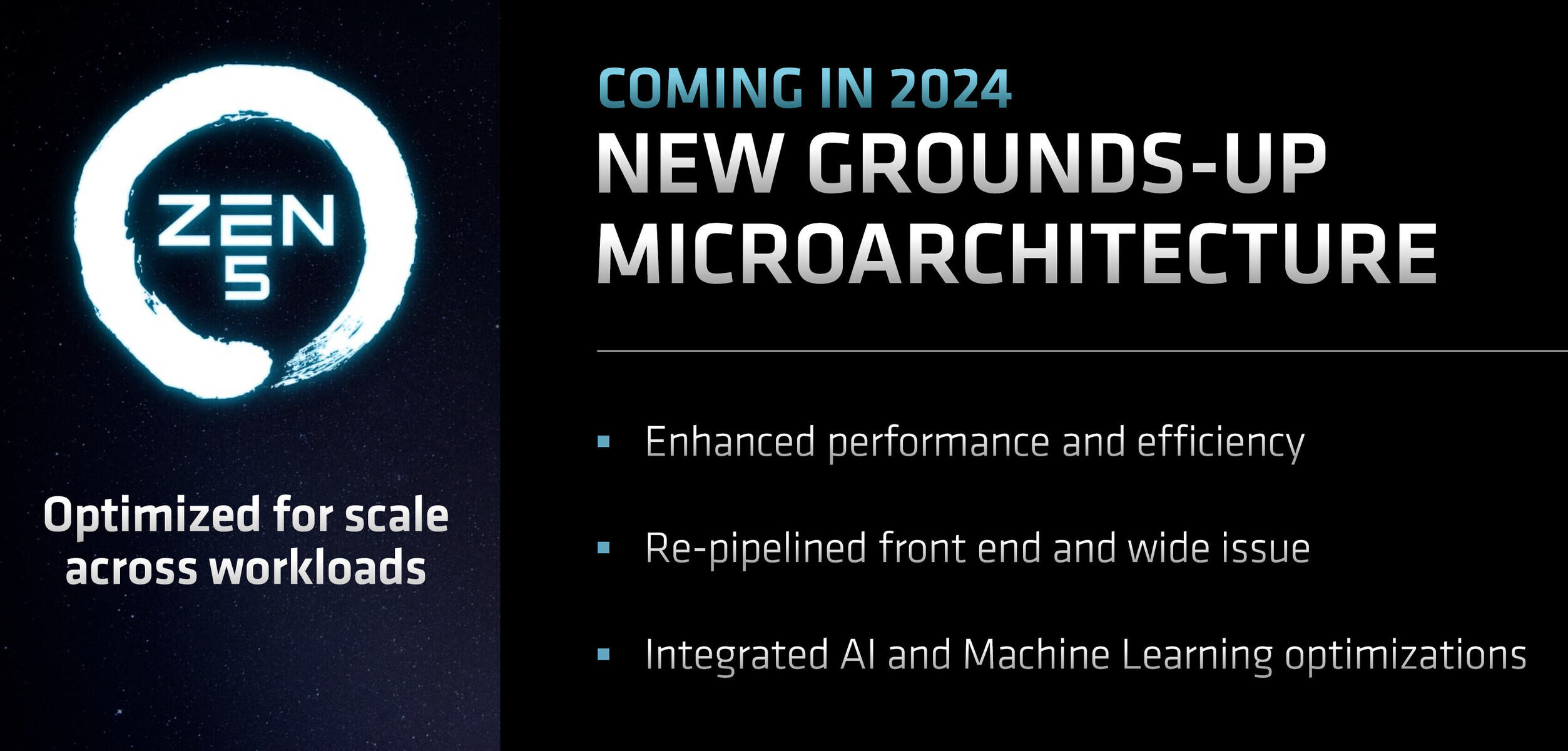
More AMD Ryzen 9000 "Zen 5" Desktop Processor Details Emerge

AMD is looking to debut its Ryzen 9000 series "Granite Ridge" desktop processors based on the "Zen 5" microarchitecture some time around May-June 2024, according to High Yield YT, a reliable source with AMD leaks. These processors will be built in the existing Socket AM5 package, and be compatible with all existing AMD 600 series chipset motherboards. It remains to be seen if AMD debuts a new line of motherboard chipsets. Almost all Socket AM5 motherboards come with the USB BIOS flashback feature, which means motherboards from even the earliest production batches that are in the retail channel, should be able to easily support the new processors.

AMD is giving its next-gen desktop processors the Ryzen 9000 series processor model numbering, as it used the Ryzen 8000 series for its recently announced Socket AM5 desktop APUs based on the "Hawk Point" monolithic silicon. "Granite Ridge" will be a chiplet-based processor, much like the Ryzen 7000 series "Raphael." In fact, it will even retain the same 6 nm client I/O die (cIOD) as "Raphael," with some possible revisions made to increase its native DDR5 memory frequency (up from the current DDR5-5200), and improve its memory overclocking capabilities. It's being reported that DDR5-6400 could be the new "sweetspot" memory speed for these processors, up from the current DDR5-6000.

AMD Zen 5 Microarchitecture Referenced in Leaked Slides

A couple of slides from AMD's internal presentation were leaked to the web by Moore's Law is Dead, referencing what's allegedly the next-generation "Zen 5" microarchitecture. Internally, the performance variant of the "Zen 5" core is referred to as "Nirvana," and the CCD chiplet (CPU core die) based on "Nirvana" cores, is codenamed "Eldora." These CCDs will make up either the company's Ryzen "Granite Ridge" desktop processors, or EPYC "Turin" server processors. The cores themselves could also be part of the company's next-generation mobile processors, as part of heterogenous CCXs (CPU core complex), next to "Zen 5c" low-power cores.

In broad strokes, AMD describes "Zen 5" as introducing a 10% to 15% IPC increase over the current "Zen 4." The core will feature a larger 48 KB L1D cache, compared to the current 32 KB. As for the core itself, it features an 8-wide dispatch from the micro-op queue, compared to the 6-wide dispatch of "Zen 4." The integer execution stage gets 6 ALUs, compared to the current 4. The floating point unit gets FP-512 capabilities. Perhaps the biggest announcement is that AMD has increased the maximum cores per CCX from 8 to 16. At this point we don't know if it means that "Eldora" CCD will have 16 cores, or whether it means that the cloud-specific CCD with 16 "Zen 5c" cores will have 16 cores within a single CCX, rather than spread across two CCXs with smaller L3 caches. AMD is leveraging the TSMC 4 nm EUV node for "Eldora," the mobile processor based on "Zen 5" could be based on the more advanced TSMC 3 nm EUV node.

AMD Ryzen 8000 "Granite Ridge" Zen 5 Processor to Max Out at 16 Cores

AMD's next-generation Ryzen 8000 "Granite Ridge" desktop processor based on the "Zen 5" microarchitecture, will continue to top out at 16-core/32-thread as the maximum CPU core-count possible, says a report by PC Games Hardware. The processor will retain the chiplet design of the current Ryzen 7000 "Raphael" processor, with two 8-core "Zen 5" CCDs, and one I/O die. It's very likely that AMD will reuse the same 6 nm client I/O die (cIOD) as "Raphael," just the way it used the same 12 nm cIOD between Ryzen 3000 "Matisse" and Ryzen 5000 "Vermeer;" but with updates that could enable higher DDR5 memory speeds. Each of the up to two "Eldora" Zen 5 CCDs has 8 CPU cores, with 1 MB of dedicated L2 cache per core, and 32 MB of shared L3 cache. The CCDs are very likely to be built on the TSMC 3 nm EUV silicon fabrication process.

Perhaps the most interesting aspect of the PCGH leak would have to be the TDP numbers being mentioned, which continue to show higher-performance SKUs with 170 W TDP, and lower tiers with 65 W TDP. With its CPU core-counts not seeing increases, AMD would bank on not just the generational IPC increase of its "Zen 5" cores, but also max out performance within the power envelope of the new node, by dialing up clock speeds. AMD could ride out 2023 with its Ryzen 7000 "Zen 4" processors on the desktop platform, with "Granite Ridge" slated to enter production only by Q1-2024. The company could update its product stack in the meantime, perhaps even bring the 4 nm "Phoenix" monolithic APU silicon to the Socket AM5 desktop platform. Ryzen 8000 is expected to retain full compatibility with existing Socket AM5, and AMD 600-series chipset motherboards.

AMD Zen 5 "Nirvana" and Zen 6 "Morpheus" Core Codenames Leaked, Confirm Foundry Nodes

An AMD engineer inadvertently leaked the core codenames of the company's upcoming "Zen 5" and "Zen 6" microarchitectures. It's important to understand here what has been leaked. "Zen 5" and "Zen 6" are microarchitecture names, just like the current "Zen 4" and past "Zen 3" or older. AMD uses codenames for the CCD (CPU complex dies) based on these microarchitectures, which it shares between Ryzen client and EPYC enterprise processors. For example, the CCD codename for "Zen 3" is "Brekenridge," and for "Zen 4" it is "Durango." AMD also uses codenames for the CPU cores themselves. "Zen 3" CPU cores are codenamed "Cerebrus," and "Zen 4" CPU cores "Persphone." And now, the leak:

The CCD based on the upcoming "Zen 5" microarchitecture is codenamed "Eldora," and the "Zen 5" CPU core itself is codenamed "Nirvana." There's no codename for the CCD based on "Zen 6," but its CPU cores are codenamed "Morpheus." The "Zen 5" microarchitecture will be based on the 3 nm EUV foundry node; while "Zen 6" will be 2 nm EUV. The engineer in the screenshot is contributing to the power-management technology behind "Zen 5" and "Zen 6," and states that their work on "Zen 5" spanned January-December of 2022, which means the development phase of the next "Zen" architecture is probably complete, and the architecture is undergoing testing and refinement. It's also claimed that work on at least the power-management aspect of "Zen 6" has started from January 2023.

Plextor at CES 2020: M9P Plus AIC SSD and its M.2 Twin

Plextor showed off its very recently announced M9P line of premium PCI-Express NVMe SSDs at CES 2020. The M9P Plus comes in both half-height add-in card (AIC) form-factor, and a more conventional M.2-2280 form-factor. In both, it leverages PCI-Express 3.0 x4 along with the NVMe 1.3 protocol. At the heart of these drives is the Marvell 88SS1092 "Eldora Plus" controller that has 8 flash channels. This controller is paired with Kioxia 96-layer 3D TLC NAND flash (BiCS 4), and a DDR4 DRAM cache.

With capacities of 256 GB, 512 GB, and 1 TB, the M9P offers sequential reads of up to 3,400 MB/s, with up to 2,200 MB/s writes (up to 1,700 MB/s writes for the 256 GB variant). Endurance (TBW) for the three models are proportionately rated at 160 TB, 320 TB, and 640 TB. The 256 GB variant of the M.2-2280 model is priced at $51, the 512 GB variant at $81, and the 1 TB variant at $135. The AIC equivalents are priced at roughly $15 premiums over these prices, and in addition to the convenience of AIC (easier to swap in a test bench), they feature some RGB LED embellishments.

Marvell's Ready to launch QLC Controller Delivers 670K IOPS

QLC is the next big step in flash memory, with another bump in density increases and, crucially for consumers, revised, lower pricing for flash-based products that employ the new technology. We've already had a sneak peek at what QLC-based products can deliver - Intel's leaked SSD 660P employs QLC memory and is expected to deliver 1,800 MB/s in sequential read and up to 1,200 MB/s in sequential write speeds with 150,000 IOPS. Expect base drive capacities to increase - QLC being higher density would mean fewer NAND chips, but manufacturers want to keep the added performance of chip parallelism.

However, flash needs controllers to deliver its true potential, and Marvell has one up its sleeve. The new controller will eventually replace the NVMe 1.1 Eldora (88SS1093) used in some popular SSDs that are already shipping, such as Plextor's M9Pe, and the folks at Tom's hardware took a peek at it - running the current TLC memory, that is. The controller delivered over 670,000 IOPS and 3,500 MB/s in the demo, though there's no information on the density of the drive. But for those performance levels, it must've had a good amount of silicon. While not representative of final QLC memory performance of the controller, it's good to know that at least this part of the ecosystem is good to go. Now if only QLC was quick and hot off the presses, we could see a $100 512 GB SSD.

Plextor Details Release Availability of their M8Se NVMe TLC SSDs

At CES 2017, Plextor announced their next SSD product line. Dubbed the M8Se, these will be restricted to NVMe SSDs with 15nm 3-bit-per-cell TLC of Toshiba manufacture, ranging from 128 GB, 256 GB, 512 GB and 1TB capacities leveraged by Marvell's Eldora controller.

The new mid-range NVMe SSD uses a new heatsink design (slight cost-reduction when compared with the one the M8Pe carries), that Plextor says will improve cooling by up to 20% - convenient, since throttling does happen with NVMe based SSDs - and particularly with Marvell's Eldora controller - as it did with Plextor's M8Pe line of SSDs. The card also features blue accent lighting. Plextor will also sell a heatsink-less M8PeGN model in the M.2 form factor.
Return to Keyword Browsing
Apr 25th, 2024 11:52 EDT change timezone

New Forum Posts

Popular Reviews

Controversial News Posts