News Posts matching #ExaFLOP

Return to Keyword Browsing

Huawei Prepares 160,000 Ascend 950DT Accelerators for DeepSeek Data Center

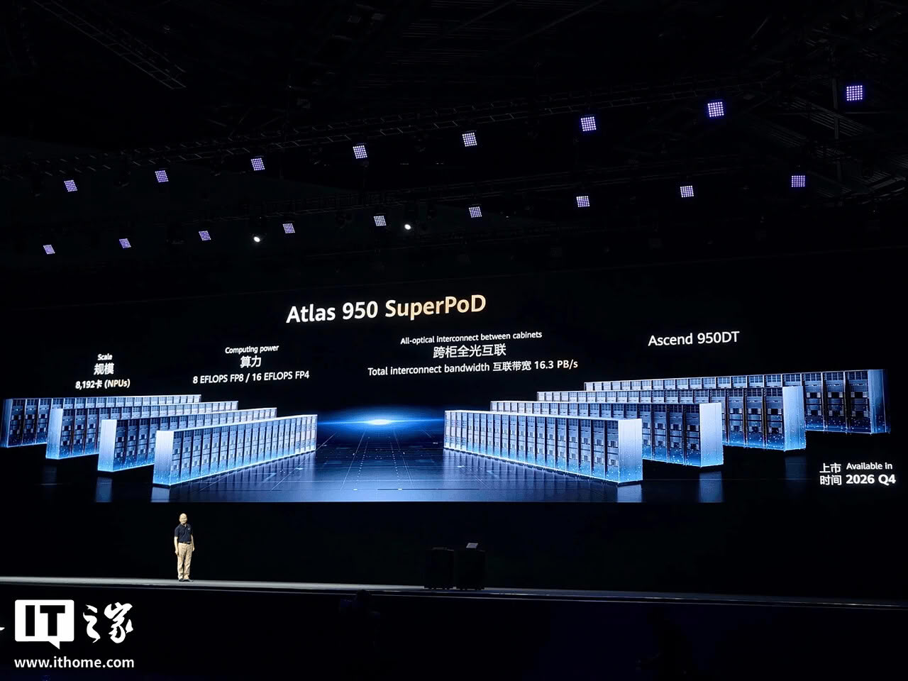
Chinese AI labs are increasingly ordering domestic AI accelerators, and one of the leading AI labs, DeepSeek, has reportedly placed an order for 160,000 Huawei Ascend 950DT chips. Late last year, Huawei revealed that the company is preparing a series of chips and rack-scale solutions to meet domestic AI demand, and now we are seeing large orders starting to materialize. For reference, the Huawei Ascend 950DT AI accelerator has a memory capacity of 144 GB, built on Huawei's own HBM memory design. This in-house solution delivers a bandwidth of nearly 4 TB/s, aligning perfectly with Huawei's vision. The chip can achieve about one PetaFLOP of FP8 peak compute, or about two PetaFLOPS of FP4.

DeepSeek, one of the leading Chinese AI labs, will use Huawei's Ascend 950DT chips for large-scale inference operations and will deploy them in a single data center located in Inner Mongolia. The overall system will deliver a peak of 160 ExaFLOPS at FP8 or about 320 ExaFLOPS at FP4 precision. The system will also have about 23 PB of total HBM memory, meaning that the large-scale inferencing operations will be able to serve thousands of customers concurrently without any issues.

Fujitsu Showcases "MONAKA" CPU Sample with 3.5D XDSiP Packaging

During MWC, Fujitsu partnered with networking equipment maker 1FINITY to unveil the first silicon wafers and an engineering sample of its "MONAKA" CPU. Scheduled for release in 2027, the initial Fujitsu MONAKA CPU utilizes the Armv9-A architecture and a 3D chiplet layout that combines a core die with separate SRAM and I/O dies. A single chip features 144 cores, and two-socket configurations can scale up to 288 cores per node. The platform supports 12-channel DDR5, PCIe 6.0 with CXL 3.0, and Arm SVE2 for AI and HPC workloads. Fujitsu has chosen TSMC to manufacture this chip using the 2 nm node, paired with Broadcom's 3.5D eXtreme Dimension System-in-Package (XDSiP) packaging architecture. This packaging allows MONAKA to become a 144-core design featuring four 36-core chiplets. These chiplets are stacked face-to-face with SRAM tiles through hybrid copper bonding, utilizing TSMC's N5 process for the cache layer.

In the pictures below, we can see the silicon complex in its early sample packaging, which shows a large central I/O die, HBM memory around the CPU, and the new packaging technology. Reportedly, this CPU has already reached a working version, with Broadcom shipping the CPU to Fujitsu in late February this year. After initial testing and early performance validation, Fujitsu plans to ship these processors to customers around summer, with mass shipping to commence in 2027. The company envisions this SoC as a powerhouse for AI inference, simulation, and large-scale data processing. It will sell these systems to external customers, who showed great interest in Fujitsu's A64FX when the Fugaku computer came online. Fugaku was the most powerful supercomputer back in 2020, achieving 415.53 PetaFLOPS of FP64 and an impressive HPL-AI score of 1.421 ExaFLOPS using lower FP16 precision. Hence, we expect the new MONAKA CPU to enable much greater speeds and some efficiency improvements as well.

NVIDIA's "Vera Rubin" Superchip System Pictured for the First Time

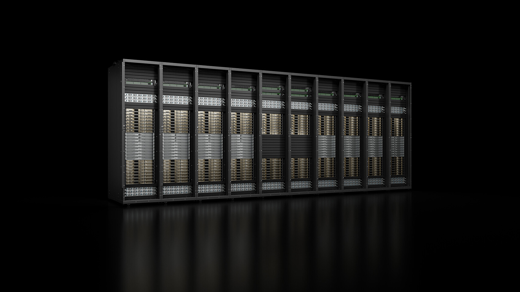
NVIDIA yesterday had a GTC conference in Washington D.C., showing its latest "Vera Rubin" Superchip symbiote. Pictured for the first time is the combination of two "Rubin" GPU paired with a single "Vera" CPU carrying 88 custom NVIDIA cores and 176 threads in a single package. NVIDIA quoted performance targets of roughly 50 PetaFLOPS of FP4 compute per Rubin GPU, which yields about 100 PetaFLOPS FP4 for the two-GPU Superchip. The company said engineering samples are already moving through labs and set mass production goals for 2026 with broader shipments and deployments into 2027.

Each Rubin GPU appears to integrate two reticle-sized compute chiplets (2x830mm²?) paired with eight HBM4 stacks, delivering about 288 GB of HBM4 per GPU and roughly 576 GB of HBM4 on the full Superchip. NVIDIA also populated the board with SOCAMM2 LPDDR5X modules to provide large, low-latency system memory, with some older briefings indicating around 1.5 TB of LPDDR5X per Vera CPU on typical trays. The Vera CPU itself uses an 88-core, 176-thread Arm-based custom design and shows signs of a multi-chiplet layout with a distinct I/O chiplet nearby. With "Grace," NVIDIA relied on Arm's Neoverse design, but with Vera, the design team brought this CPU core in the house to extract maximum performance. Additionally, NVLink bandwidth climbs to approximately 1.8 TB/s to sustain heavy CPU-to-GPU traffic in system-demanding workloads such as AI inference and training.

NVIDIA Unveils "Rubin CPX" GPU: Single-Die, 30 PetaFLOPS, and 128 GB of GDDR7 Memory

During the AI Infra Summit, NVIDIA announced the "Rubin CPX" GPU, a specialized accelerator derived from the upcoming "Rubin" family, specifically made for massive-context AI models. The chip delivers 30 PetaFLOPS of NVFP4 compute performance on a monolithic die, accompanied by 128 GB of GDDR7 memory. The monolithic die configuration represents a departure from the dual-GPU packages characteristic of NVIDIA's current Blackwell and Blackwell Ultra architectures, as well as the design path that the rest of the Rubin family will follow. The Rubin CPX addresses computational bottlenecks in extended-context scenarios where AI models process millions of tokens simultaneously. This capability proves critical for applications including comprehensive software codebase analysis and hour-long video content processing, which can require up to one million tokens.

The processor integrates four NVENC and four NVDEC video encoders directly on-chip, enabling streamlined multimedia workflows without external processing dependencies. Performance metrics suggest that the Rubin CPX is delivering three times the attention processing speed of NVIDIA's current best GB300 Blackwell Ultra accelerator systems. The architecture employs a cost-optimized single-die approach, rather than multi-chip modules, which potentially reduces manufacturing complexity while maintaining computational density. Memory bandwidth specifications remain undisclosed, though a 512-bit interface could yield approximately 1.8 TB/s throughput when using 30 Gbps GDDR7 memory chips. NVIDIA plans integration of Rubin CPX processors within the Vera Rubin NVL144 CPX platform, which combines traditional Rubin GPUs with the specialized CPX variants. This hybrid configuration targets 8 ExaFLOPS of aggregate compute performance, with 1.7 PB/s of memory bandwidth, across a complete rack deployment. The "Kyber" rack will include ConnectX-9 network adapters capable of 1600G networking, Spectrum6 doing 102.4T switching, as well as co-packaged optics. NVIDIA plans this to arrive in late 2026, after the regular Rubin GPU launch in early 2026.

Jupiter Boots Up: Europe's Fastest Supercomputer Runs on NVIDIA Grace Hopper

Europe's high-performance computing sector received a significant boost today as the Jupiter supercomputer was officially powered on at the Jülich Supercomputing Center. The modular exascale system delivers a peak of nearly one ExaFLOP (930 PetaFLOPS) of FP64 performance and debuts as the fastest machine in Europe, positioned at number four on the Top500 list. Built around NVIDIA Grace Hopper technology, the booster contributes approximately 793 PetaFLOPs of FP64, while each compute node features four GH200 accelerators, resulting in a fleet of 23,752 accelerators across 5,938 nodes, all mounted in 125 server racks. Those GH200-class accelerators are noted for their strong energy efficiency, with published figures of nearly 60.5 GigaFLOPS per watt, and an accelerator farm drawing on the order of double-digit megawatts of power. Jupiter is primarily designed for AI workloads. Hence, it delivers over 90 ExaFLOPS in AI's favorite FP8 format.

Reported build costs are estimated to be near €500 million, and European planners anticipate a multibillion-euro expansion will be required to close capacity gaps, with figures of around €60 billion cited for deployments through 2030. Planners envision roughly 13 specialized AI data centers and gigafactory-scale facilities, with Jülich a candidate for expansion. Backers say this is about digital sovereignty, keeping critical infrastructure close to European research and industry rather than depending on foreign cloud providers. Operationally, Jupiter will support climate modelling, materials simulation and biological research, complemented by an inference module, Jarvis, for fast model serving. For Europe, Jupiter is meant to be both a capability and a signal: an energy-conscious exascale platform designed to anchor AI work and catalyze further regional investment.

Safe Superintelligence Inc. Uses Google TPUs Instead of Regular GPUs for Next-Generation Models

It seems like Google aims to grab a bit of the market share from NVIDIA and AMD by offering startups large compute deals and allowing them to train their massive AI models on the Google Cloud Platform (GCP). One such case is the OpenAI co-founder Ilya Sutskever's Safe Superintelligence Inc. (SSI) startup. According to a GCP post, SSI is "partnering with Google Cloud to use TPUs to accelerate its research and development efforts toward building a safe, superintelligent AI." Google's latest TPU v7p, codenamed Ironwood, was released yesterday. Carrying 4,614 TeraFLOPS of FP8 precision and 192 GB of HBM memory, these TPUs are interconnected using Google's custom ICI infrastructure and are scaled to configurations in pods of 9,216 chips, where Ironwood delivers 42.5 ExaFLOPS of total computing power.

For AI training, this massive power will allow AI models to quickly go over training, accelerating research iterations and ultimately accelerating model development. For SSI, the end goal is a simple mission: achieving ASI with safety at the front. "We approach safety and capabilities in tandem, as technical problems to be solved through revolutionary engineering and scientific breakthroughs. We plan to advance capabilities as fast as possible while making sure our safety always remains ahead," notes the SSI website, adding that "Our singular focus means no distraction by management overhead or product cycles, and our business model means safety, security, and progress are all insulated from short-term commercial pressures."

Japan Unveils Plans for Zettascale Supercomputer: 100 PFLOPs of AI Compute per Node

The zettascale era is officially on the map, as Japan has announced plans to develop a successor to its renowned Fugaku supercomputer. The Ministry of Education, Culture, Sports, Science and Technology (MEXT) has set its sights on creating a machine capable of unprecedented processing power, aiming for 50 ExaFLOPS of peak AI performance with zettascale capabilities. The ambitious "Fugaku Next" project, slated to begin development next year, will be headed by RIKEN, one of Japan's leading research institutions, in collaboration with tech giant Fujitsu. With a target completion date of 2030, the new supercomputer aims to surpass current technological boundaries, potentially becoming the world's fastest once again. MEXT's vision for the "Fugaku Next" includes groundbreaking specifications for each computational node.

The ministry anticipates peak performance of several hundred FP64 TFLOPS for double-precision computations, around 50 FP16 PFLOPS for AI-oriented half-precision calculations, and approximately 100 PFLOPS for AI-oriented 8-bit precision calculations. These figures represent a major leap from Fugaku's current capabilities. The project's initial funding is set at ¥4.2 billion ($29.06 million) for the first year, with total government investment expected to exceed ¥110 billion ($761 million). While the specific architecture remains undecided, MEXT suggests the use of CPUs with special-purpose accelerators or a CPU-GPU combination. The semiconductor node of choice will likely be a 1 nm node or even more advanced nodes available at the time, with advanced packaging also used. The supercomputer will also feature an advanced storage system to handle traditional HPC and AI workloads efficiently. We already have an insight into Monaka, Fujitsu's upcoming CPU design with 150 Armv9 cores. However, Fugaku Next will be powered by the Monaka Next design, which will likely be much more capable.

AWS and NVIDIA Partner to Deliver 65 ExaFLOP AI Supercomputer, Other Solutions

Amazon Web Services, Inc. (AWS), an Amazon.com, Inc. company (NASDAQ: AMZN), and NVIDIA (NASDAQ: NVDA) today announced an expansion of their strategic collaboration to deliver the most-advanced infrastructure, software and services to power customers' generative artificial intelligence (AI) innovations. The companies will bring together the best of NVIDIA and AWS technologies—from NVIDIA's newest multi-node systems featuring next-generation GPUs, CPUs and AI software, to AWS Nitro System advanced virtualization and security, Elastic Fabric Adapter (EFA) interconnect, and UltraCluster scalability—that are ideal for training foundation models and building generative AI applications.

The expanded collaboration builds on a longstanding relationship that has fueled the generative AI era by offering early machine learning (ML) pioneers the compute performance required to advance the state-of-the-art in these technologies.

Chinese Exascale Sunway Supercomputer has Over 40 Million Cores, 5 ExaFLOPS Mixed-Precision Performance

The Exascale supercomputer arms race is making everyone invest their resources into trying to achieve the number one spot. Some countries, like China, actively participate in the race with little proof of their work, leaving the high-performance computing (HPC) community wondering about Chinese efforts on exascale systems. Today, we have some information regarding the next-generation Sunway system, which is supposed to be China's first exascale supercomputer. Replacing the Sunway TaihuLight, the next-generation Sunway will reportedly boast over 40 million cores in its system. The information comes from an upcoming presentation for Supercomputing 2023 show in Denver, happening from November 12 to November 17.

The presentation talks about 5 ExaFLOPS in the HPL-MxP benchmark with linear scalability on the 40-million-core Sunway supercomputer. The HPL-MxP benchmark is a mixed precision HPC benchmark made to test the system's capability in regular HPC workloads that require 64-bit precision and AI workloads that require 32-bit precision. Supposedly, the next-generation Sunway system can output 5 ExaFLOPS with linear scaling on its 40-million-core system. What are those cores? We are not sure. The last-generation Sunway TaihuLight used SW26010 manycore 64-bit RISC processors based on the Sunway architecture, each with 260 cores. There were 40,960 SW26010 CPUs in the system for a total of 10,649,600 cores, which means that the next-generation Sunway system is more than four times more powerful from a core-count perspective. We expect some uArch and semiconductor node improvements as well.

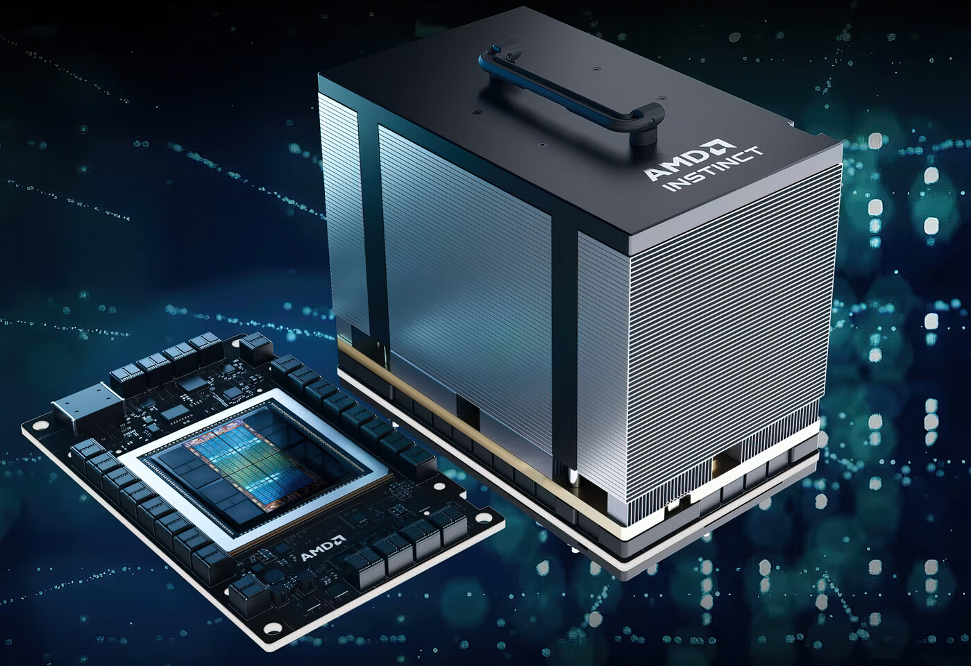
Two-ExaFLOP El Capitan Supercomputer Starts Installation Process with AMD Instinct MI300A

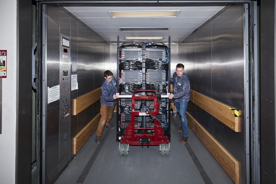
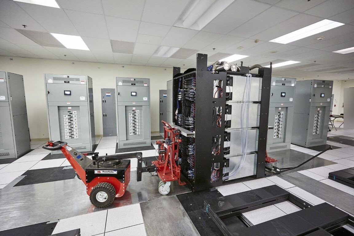
When Lawrence Livermore National Laboratory (LLNL) announced the creation of a two-ExaFLOP supercomputer named El Capitan, we heard that AMD would power it with its Instinct MI300 accelerator. Today, LNLL published a Tweet that states, "We've begun receiving & installing components for El Capitan, @NNSANews' first #exascale #supercomputer. While we're still a ways from deploying it for national security purposes in 2024, it's exciting to see years of work becoming reality." As published images show, HPE racks filled with AMD Instinct MI300 are showing up now at LNLL's facility, and the supercomputer is expected to go operational in 2024. This could mean that November 2023 TOP500 list update wouldn't feature El Capitan, as system enablement would be very hard to achieve in four months until then.

The El Capitan supercomputer is expected to run on AMD Instinct MI300A accelerator, which features 24 Zen4 cores, CDNA3 architecture, and 128 GB of HBM3 memory. All paired together in a four-accelerator configuration goes inside each node from HPE, also getting water cooling treatment. While we don't have many further details on the memory and storage of El Capitan, we know that the system will exceed two ExFLOPS at peak and will consume close to 40 MW of power.

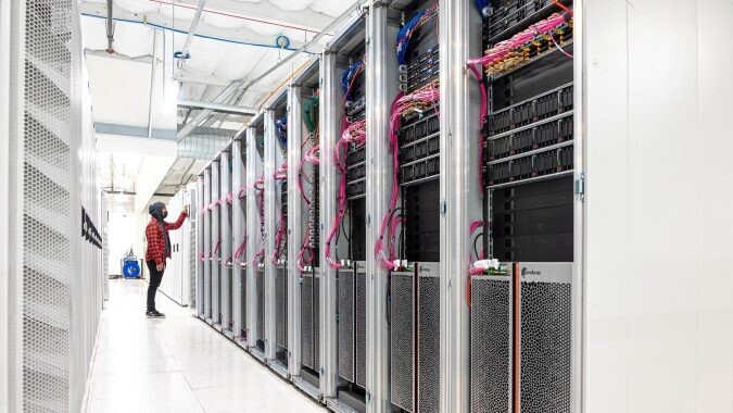
Cerebras Unveils Andromeda, a 13.5 Million Core AI Supercomputer that Delivers Near-Perfect Linear Scaling for Large Language Models

Cerebras Systems, the pioneer in accelerating artificial intelligence (AI) compute, today unveiled Andromeda, a 13.5 million core AI supercomputer, now available and being used for commercial and academic work. Built with a cluster of 16 Cerebras CS-2 systems and leveraging Cerebras MemoryX and SwarmX technologies, Andromeda delivers more than 1 Exaflop of AI compute and 120 Petaflops of dense compute at 16-bit half precision. It is the only AI supercomputer to ever demonstrate near-perfect linear scaling on large language model workloads relying on simple data parallelism alone.

With more than 13.5 million AI-optimized compute cores and fed by 18,176 3rd Gen AMD EPYC processors, Andromeda features more cores than 1,953 Nvidia A100 GPUs and 1.6 times as many cores as the largest supercomputer in the world, Frontier, which has 8.7 million cores. Unlike any known GPU-based cluster, Andromeda delivers near-perfect scaling via simple data parallelism across GPT-class large language models, including GPT-3, GPT-J and GPT-NeoX.
Return to Keyword Browsing
Nov 11th, 2026 18:31 CST change timezone

New Forum Posts

Popular Reviews

TPU on YouTube

Controversial News Posts