News Posts matching #Fire Strike

Return to Keyword Browsing

Intel Core Ultra 5 125H Squares off Against AMD Ryzen 7 7840HS in Benchmark Leak

The Intel Core Ultra 5 125H is designed to be a middle-of-the-market processor SKU from Intel's next generation "Meteor Lake" processor family. It comes with a CPU core configuration of 14-core/18-thread. That's 4P+8E+2L (four performance cores, eight efficiency cores, two low-power island cores), although with a full featured Xe-LPG iGPU that has all 8 Xe cores (128 EU) enabled. The chip is normally rated for a 28 W power envelope, although OEMs such as Lenovo have developed a custom 65 W "power mode," which raises the base power value.

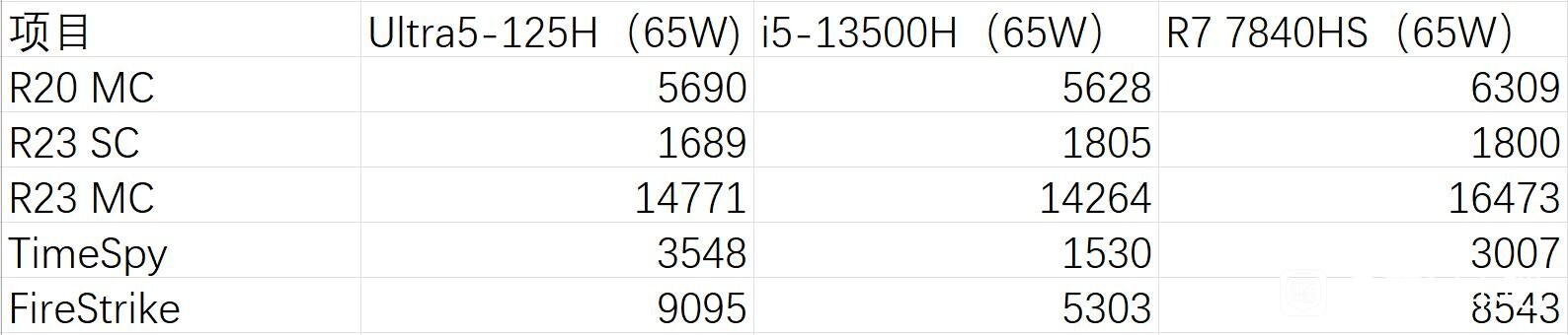
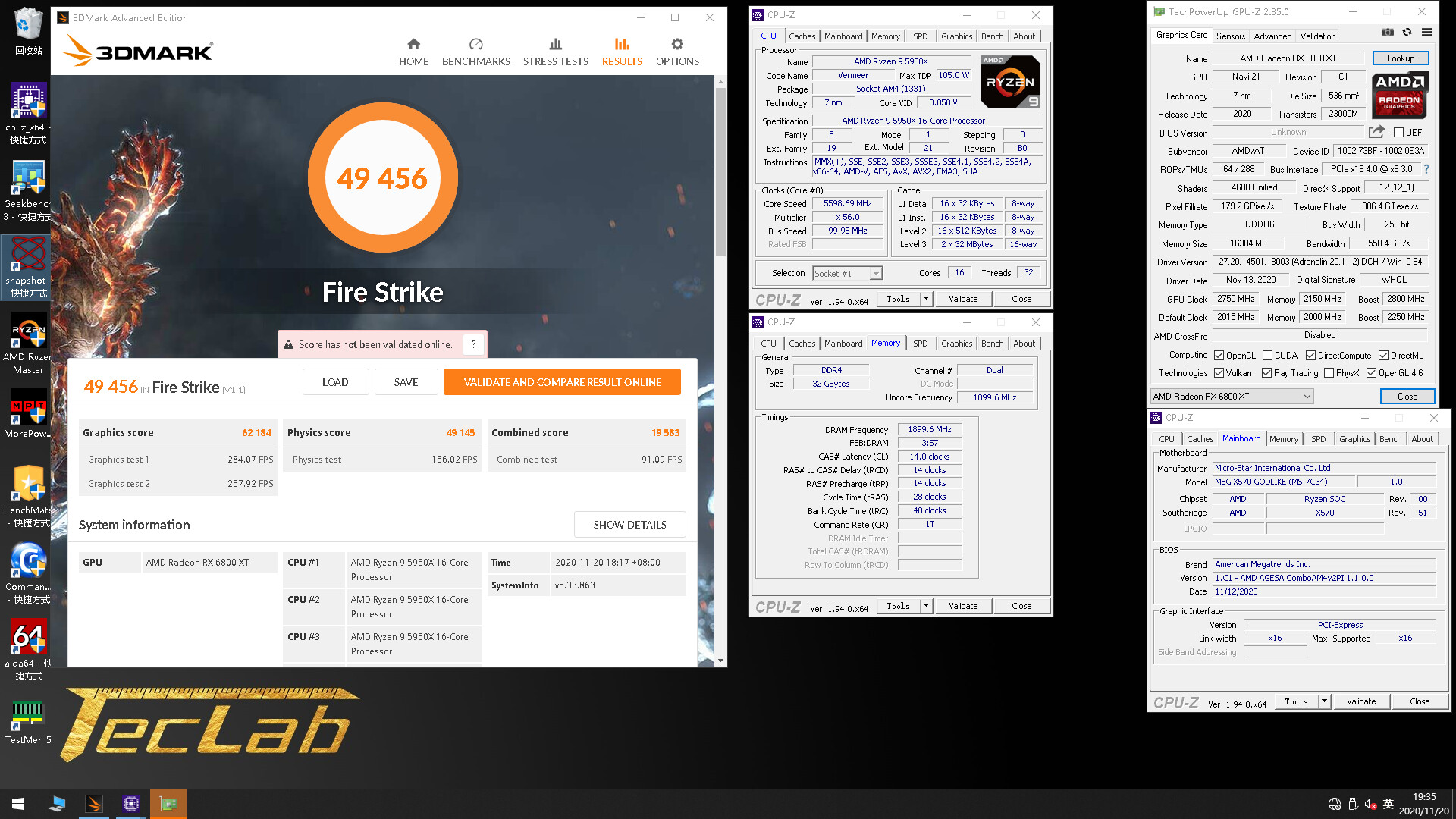
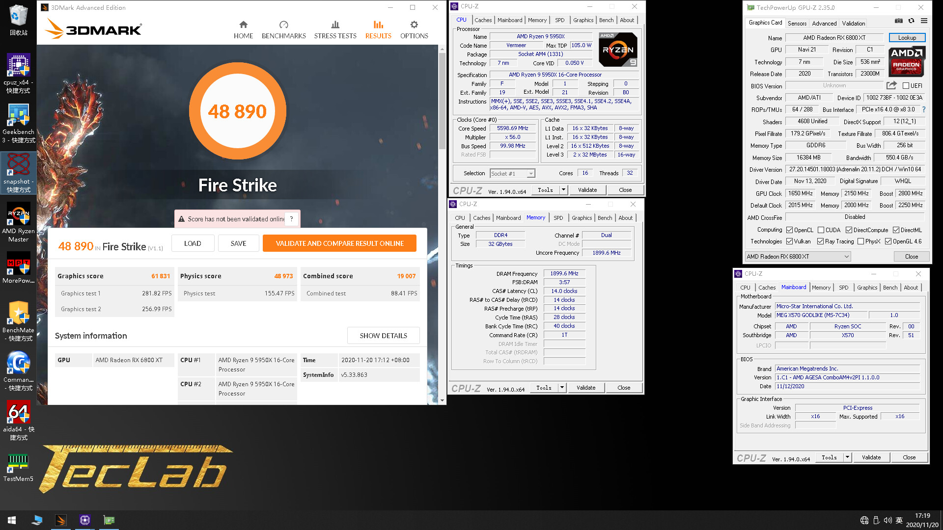
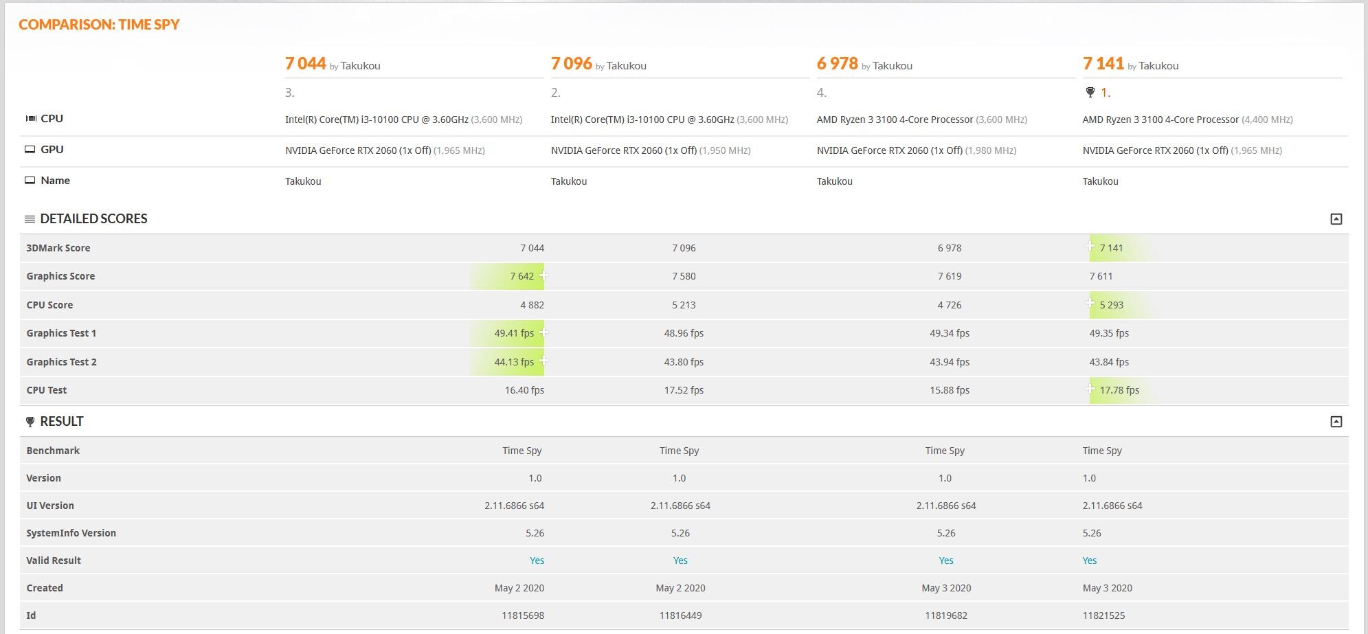
A Chinese PC enthusiast with access to an unreleased Lenovo notebook based on this processor, including Lenovo's 65 W Mode toggle, benchmarked it, and compared it with a notebook powered by an AMD Ryzen 7 7840HS "Phoenix" processor (8-core/16-thread, "Zen 4," Radeon 780M iGPU with all 12 compute units enabled); and another notebook powered by Intel's current middle-of-market chip in the H-segment, the Core i5-13500H "Raptor Lake" (4P+8E, Xe-LP iGPU with 5 Xe cores or 80 EU). The results were a little unexpected. The Xe-LPG iGPU of the 125H is shown beating both the Radeon 780M of the Ryzen, and the Xe-LP iGPU of the i5-13500H, with the highest 3DMark Time Spy and Fire Strike scores in the comparison. The Xe-LPG iGPU is 15% faster than the Radeon 780M in Time Spy, and 6% faster in Fire Strike. It's a whopping 70% faster than the Xe-LP iGPU of the "Raptor Lake" chip in this comparison. Things are shockingly different on the CPU performance front for the "Meteor Lake" chip.

Intel Arc A550M & A770M 3DMark Scores Surface

The upcoming Intel Arc A550M & A770M mobile graphics cards have recently appeared on 3DMark in Time Spy and Fire Strike Extreme. The Intel Arc Alchemist A550M features an ACM-G10 GPU with 16 Xe cores paired with 8 GB of GDDR6 memory on a 128-bit bus while the A770M features the same GPU but with 32 Xe cores and 16 GB of GDDR6 memory on a 256-bit bus.

The A550M was tested in 3DMark Time Spy where it scored 6017 points running on an older 1726 driver with Intel Advanced Performance Optimizations (APO) enabled. The A770M was benchmarked with 3DMark Fire Strike Extreme where it scored a respectable 13244 points in graphics running on test drivers which places it near the RTX 3070M. This score does not correlate to real-world gaming performance with figures provided directly by Intel showing the Arc A730M only being 12% faster than the RTX 3060M.

First Intel Arc A730M Powered Laptop Goes on Sale, in China

The first benchmark result of an Intel Arc A730M laptop made an appearance online and the mysterious laptop used to run 3DMark turned out to be from a Chinese company called Machenike. The laptop itself appears to go under the name of Dawn16 Discovery Edition and features a 16-inch display with a native resolution of 2560 x 1600, with a 165 Hz refresh rate. CPU wise, Machenike went with a Core i7-12700H, which is a 6+8 core CPU with 20 threads, where the performance cores top out at 4.7 GHz. The CPU has been paired with 16 GB of 4800 MHz DDR5 memory and the system also has a PCIe 4.0 NVMe SSD of some kind, with a max read speed of 3500 MB/s, which isn't particularly impressive. Other features include Thunderbolt 4 support, WiFi 6E and Bluetooth 5.2, as well as an 80 Whr battery pack.

However, none of the above is particularly unique and what matters here is of course the Intel Arc A730M GPU. It has been paired with 12 GB of GDDR6 memory with a 192-bit interface, at 14 Gbps according to the specs. The memory bandwidth is said to be 336 GB/s. The company also provided a couple of performance metrics, with a 3DMark TimeSpy figure of 10002 points and a 3DMark Fire Strike figure of 23090 points. The TimeSpy score is a few points slower than the numbers posted earlier, but helps verify the earlier test result. Other interesting nuggets of information include support for 8k60 12-bit HDR video decoding for AV1, HEVC, AVC and VP9, as well as 8k 10-bit HDR encoding for said formats. Here a figure for the Puget Benchmark in what appears to be Photoshop (PS) is provided, where it scores 1188 points. The laptop is up for what appears to be pre-order, with a price tag of 7,499 RMB, or about US$1,130.

AMD Radeon RX 6900 XT Scores Top Spot in 3DMark Fire Strike Hall of Fame with 3.1 GHz Overclock

3DMark Fire Strike Hall of Fame is where overclockers submit their best hardware benchmark trials and try to beat the very best. For years, one record managed to hold, and today it just got defeated. According to an extreme overclocker called "biso biso" from South Korea and a part of the EVGA OC team, the top spot now belongs to the AMD Radeon RX 6900 XT graphics card. The previous 3DMark Fire Strike world record was set on April 22nd in 2020, when Vince Lucido, also known as K|NGP|N, set a record with four-way SLI of NVIDIA GeForce GTX 1080 Ti GPUs. However, that record is old news since January 27th, when biso biso set the history with AMD Radeon RX 6900 XT GPU.

The overclocker scored 62389 points, just 1,183 more from the previous record. He pushed the Navi 21 XTX silicon that powers the Radeon RX 6900 XT card to an impressive 3,147 MHz. Paired with a GPU memory clock of 2370 MHz, the GPU was probably LN2 cooled to achieve these results. The overclocker used EVGA's Z690 DARK KINGPIN motherboard with Intel Core i9-12900K processor as a platform of choice to achieve this record. You can check it out on the 3DMark Fire Strike Hall of Fame website to see yourself.

Intel Core i9-11900KB Beast Canyon NUC 11 Extreme Benchmarked

We now have preliminary benchmarks for the unreleased NUC 11 Extreme Beast Canyon NUC in 3DMark. We have already seen various leaks of the upcoming device detailing the available configurations and options. The NUC 11 Extreme will be offered with a choice of four processors with the highest being the upcoming Intel Core i9-11900KB which is the star of today's benchmarks. The i9-11900KB equipped NUC was paired with a desktop RTX 3060 and was put through its paces in the Fire Strike and Time Spy 3DMark benchmarks. The i9-11900KB is a specialty processor designed for use in NUC products with the new add-in card form factor and is largely comparable to the desktop i9-11900.

The Intel Core i9-11900KB is an 8 core 16 thread mobile processor with a base clock of 3.3 GHz, a boost clock of 4.9 GHz and a thermal velocity boost of 5.3 GHz. The chip features 24 MB of L3 cache and comes with a configurable TDP of 55 W/65 W. The base clock is higher than the 2.5 GHz found on the desktop i9-11900 while the boost clock is 300 MHz less and the thermal velocity boost is 100 MHz higher. The Intel Core i9-11900KB averages 93% - 101% of the performance of the i9-11900 which is to be expected considering the clock speeds.

Intel Xe HPG Graphics Card Could Compete with Big Navi & Ampere

Intel started shipping their first Xe DG1 graphics card to OEMs earlier this year which features 4 GB of LPDDR4X and 80 execution units. While these initial cards aren't high performance and only compete with entry-level products like the NVIDIA MX350 they demonstrated Intel's ability to produce a discrete GPU. We have recently received some more potential performance information about Intel's next card the DG2 from chief GPU architect, Raja Koduri. Koduri posted an image of him with the team at Intel's Folsom lab working on the Intel Iris Pro 5200 iGPU back in 2012 and noted that now 9 years later their new GPU is over 20 times faster. The Intel Iris Pro 5200 scores 1015 on Videocard Benchmarks and ~1,400 points on 3DMark Fire Strike, if we assume these scores will be 20x more we get values of ~20,300 in Videocard Benchmarks and 28,000 points in Fire Strike. While these values don't extrapolate perfectly they provide a good indication of potential performance placing the GPU in the same realm of the NVIDIA RTX 3070 and AMD RX 6800.

3.00 GHz OC Possible on AMD Radeon RX 6900 XT; RX 6800 XT Capped at 2.80 GHz

It's becoming clear that AMD's new "Big Navi" Radeon RX 6800 XT is a treat for overclockers, and that it launched with much lower engine clocks than the silicon is capable of, resulting in what is possibly the largest overclocking headroom on an AMD GPU in a long time. This has been highlighted by recent conquests of the 3DMark Fire Strike leaderboard by RX 6800 XT cards, displacing even the RTX 3090 from the top. It's becoming even more clear now just how far the RX 6800 XT can be pushed. Patrick Schur on Twitter reports that the RX 6800 XT engine clocks are capped at 2.80 GHz, which is possibly why we're yet to see anything faster than that. The upcoming RX 6900 XT, on the other hand, is a better-endowed beast.

According to Schur, the RX 6900 XT has a raised engine clocked limit to 3.00 GHz in comparison to the 2.80 GHz of the RX 6800 XT. This 200 MHz increase, coupled with the 8 additional RDNA2 compute units, should mean that the Fire Strike leaderboards will get another shake-up in December, when these cards are released to market. The memory clock on both cards is capped at 1075 MHz (real), or 17.2 Gbps GDDR6-effective, although this should depend heavily on the overclocking headroom of the memory chips. It's important to note here that neither the 3.00 GHz of the RX 6900 XT, nor the 2.80 GHz for the RX 6800 XT, are advertised clock speeds for the cards, and are achievable only by manual overclocking, in some cases employing extreme cooling solutions such as liquid nitrogen.

NVIDIA GeForce RTX 3060 Ti Fire Strike and Time Spy Scores Surface

3DMark scores of the upcoming NVIDIA GeForce RTX 3060 Ti were leaked to the web by VideoCardz. The RTX 3060 Ti was put through standard 3DMark Fire Strike and Time Spy benchmark runs. In the DirectX 11-based Fire Strike benchmark, the card allegedly scores 30706 points, with 146.05 FPS in GT1 and 122 FPS in GT2. With the newer DirectX 12-based Time Spy test, it allegedly scores 12175 points, with 80.82 FPS in GT1, and 68.71 FPS in GT2. There are no system specs on display, but the scores put the RTX 3060 Ti slightly ahead of the previous-generation high-end GeForce RTX 2080 Super.

The GeForce RTX 3060 Ti, bound for a December 2 launch, is an upcoming performance-segment graphics card based on the "Ampere" architecture, and is carved out of the same 8 nm "GA104" silicon as the RTX 3070. It reportedly packs 4,864 "Ampere" CUDA cores, 38 second-gen RT cores, 152 third-gen Tensor cores, and the same memory configuration as the RTX 3070—8 GB of 14 Gbps GDDR6 across a 256-bit wide bus. NVIDIA is targeting a "<$399" price-point, making the card at least 43% cheaper than the RTX 2080 Super.

Radeon RX 6800 XT Overclocked to 2.80 GHz on LN2, Crushes 3DMark Fire Strike Record

One of the secret sauces of AMD's new "Big Navi" Radeon RX 6800 series GPUs is the ability for the GPU to sustain high engine clock speeds, with the company leveraging boost frequencies above 2.00 GHz in certain scenarios. It was only a matter of time before professional overclockers got their hands on an RX 6800 XT, and paired it with an LN2 evaporator. TecLab_Takukou is the new king of the 3DMark Fire Strike leaderboard thanks to their skills in running an RX 6800 XT at insane 2.80 GHz engine clocks. Takukou overclocked the RX 6800 XT to 2.80 GHz core, and 2150 MHz (17.2 Gbps) memory. This particular configuration yielded a Fire Strike score of 48890 points.

In a separate feat, with the RX 6800 XT running at 2.75 GHz, Takukou chased down the HWBot 3DMark Fire Strike leaderboard, with 49456 points. For both the 2.80 GHz and 2.75 GHz feats, the rest of the system included an LN2-cooled AMD Ryzen 9 5950X processor running at 5.60 GHz all-core, 32 GB of DDR4-3800 memory, and an MSI MEG X570 GODLIKE motherboard. From the looks of it, Takukou is using a reference-design RX 6800 XT board, so we can only hope what else can be accomplished from custom-design RX 6800 XT boards, such as the Sapphire NITRO+, PowerColor Red Devil, or ASUS ROG Strix O16G. Takukou leads the 3DMark Fire Strike leaderboard, followed by another RX 6800 XT-powered close-second, Lucky_n00b (47932 points, 2.65 GHz engine clock on air). Safedisc is third (47725 points, RTX 3090 @ 2.38 GHz).

Intel 8-core/16-thread "Rocket Lake-S" Processor Engineering Sample 3DMarked

The "Rocket Lake-S" microarchitecture by Intel sees the company back-port its next-generation "Willow Cove" CPU core to the existing 14 nm++ silicon fabrication process in the form of an 8-core die with a Gen12 Xe iGPU. An engineering sample of one such processor made it to the Futuremark database. Clocked at 3.20 GHz with 4.30 GHz boost frequency, the "Rocket Lake-S" ES was put through 3DMark "Fire Strike" and "Time Spy," with its iGPU in play, instead of a discrete graphics card.

In "Fire Strike," the "Rocket Lake-S" ES scores 18898 points in the physics test, 1895 points in the graphics tests, and an overall score of 1746 points. With "Time Spy," the overall score is 605, with a CPU score of 4963 points, and graphics score of 524. The 11th generation Core "Rocket Lake-S" processor is expected to be compatible with existing Intel 400-series chipset motherboards, and feature a PCI-Express gen 4.0 root complex. Several 400-series chipset motherboards have PCIe gen 4.0 preparation for exactly this. The increased IPC from the "Willow Cove" cores is expected to make the 8-core "Rocket Lake-S" a powerful option for gaming and productivity tasks that don't scale across too many cores.

Core i3-10100 vs. Ryzen 3 3100 Featherweight 3DMark Showdown Surfaces

AMD's timely announcement of the Ryzen 3 "Matisse" processor series could stir things up in the entry-level as Intel kitted its 10th generation Core i3 processors as 4-core/8-thread. Last week, a head-to-head Cinebench comparison between the i3-10300 and 3300X ensued, and today we have a 3DMark Firestrike and Time Spy comparison between their smaller siblings, the i3-10100 and the 3100, courtesy of Thai PC enthusiast TUM_APISAK. The two were benchmarked on Time Spy and Fire Strike on otherwise constant hardware: an RTX 2060 graphics card, 16 GB of memory, and a 1 TB Samsung 970 EVO SSD.

With Fire Strike, the 3100-powered machine leads in overall 3DMark score (by 0.31%), CPU-dependent Physics score (by 13.7%), and the Physics test. The i3-10100 is ahead by 1.4% in the Graphics score thanks to a 1.6% lead in graphics test 1, and 1.4% lead in graphics test 2. Over to the more advanced Time Spy test, which uses the DirectX 12 API that better leverages multi-core CPUs, we see the Ryzen 3 3100 post a 0.63% higher overall score, 1.5% higher CPU score; while the i3-10100 powered machines post within 1% higher graphics score. These numbers may suggest that the i3-10100 and the 3100 are within striking distance of each other and that either is a good pick for gamers, until you look at pricing. Intel's official pricing for the i3-10100 is $122 (per chip in 1,000-unit tray), whereas AMD lists the SEP price of the Ryzen 3 3100 at $99 (the Intel chip is at least 22% pricier), giving AMD a vast price-performance advantage that's hard to ignore, more so when you take into account value additions such as an unlocked multiplier and PCIe gen 4.0.

AMD RX Vega 56 to Vega 64 BIOS Flash - No Unlocked Shaders, Improved Performance

A ChipHell forum user has done what probably others have already done in relative obscurity: trying (and succeeding) to flash a Vega 64 BIOS onto a Vega 56 graphics card. The result? Well, apparently the shaders won't unlock (at least not according to our very own GPU-Z), but interestingly, performance improves all the same. The lesser amount of shaders on the Vega 56 silicon (3585 Shaders / 224 TMUs / 64 ROPs compared to Vega 64's 4096 / 256 / 64 apparently doesn't hinder performance that much. It appears that the improved clockspeeds of Vega 56 after the BIOS flash do more than enough to offset performance loss from the lesser amount of compute resources available, bumping RX Vega's clock speeds of 1471 MHz core boost clock and 800 MHz HBM2 memory up to Vega 64's 1545 MHz core boost clock and 945 MHz HBM2 clock.

This means that Vega 56 can effectively become a Vega 64 in performance (at least where 3D Mark Fire Strike is concerned), which isn't unheard of in the relationship between AMD's top tier and second-best graphics cards. Now naturally, some Vega 56 samples may even be further overclocked than Vega 64's stock clocks, which means that there is the potential for Vega 56 to have even better performance than Vega 64. The BIOS swap should allow Vega 56 to access higher power states than its stock BIOS allows, which is one of the reasons it can unlock higher core and memory clocks than an overclocked, original BIOS Vega 56 would. However, the fact that a Vega 56 at Vega 64 clocks and a Vega 64 deliver around the same score in benchmarks definitely does raise questions on how well the extra computing resources of Vega 64 are being put to use.

AMD Vega 10 3DMark Fire Strike Results Surface

Another day, another set of Vega results see the light of it. It would seem like this saga has been going on for ages, ever since we've seen AMD showcase its prototype Vega cards running Star Wars Battlefront (4K, Ultra settings at over 60 FPS) and Doom (4K, Vulcan render path at over 60 FPS on pre-production hardware). But with the lack of official information coming from AMD (let's hope this changes on May 16th), it would seem the company is content to see us hardware news sites jumping at every detail and offering free publicity.

This is known to be Vega because the device ID, 687F:C1, was spotted on AMD's own hands while running that Doom demo in 4K. The device clocks seem to be in line with previous leaks: a 1200 MHz core clock and 8GB of video memory running at 700 MHz memory clocks. With these clocks (which are expected to be extremely conservative when we take into account what we know of Vega), the Vega video card manages to deliver a 17,801 points graphics score, approximately 1,400 points more than your average Fury X, but some hundreds less than your average, current-generation GTX 1070. Remember: AMD's MI25 is expected to come in at 1,500 MHz core clocks, and this is a professional, passively-cooled graphics card. This means that unless AMD greatly overestimated the clock capability of its Vega cards, the consumer version of Vega will have necessarily higher clocks. But we'll stay here, waiting for some more details to pour our way, as always.

AMD's Ryzen 7 1700X Glorious Benchmarks Leak; IHS, Pin Layout Photographed

Another day, another leak: the folks at XFastest have indeed been the fastest to leak images of an actual Ryzen 7 1700X processor, with pictures of the processor's IHS and pin area running rampant throughout the Internet (the Ryzen chip is located to the right in both pictures, with a sample of AMD's previous-generation FX CPUs on the left side for comparison sake).

While revealing shots may have their appeal, it's the benchmarking portion that most of us are expectant about. Until actual reviews are out, we're left nothing more than these leaks (which should be taken with appropriate amounts of salt). In this case, benchmarks of AMD's upcoming Ryzen 7 1700X have been released, showing just how the upcoming CPU delivers in 3D Mark Fire Strike, CPU Mark and Cinebench R15.
Return to Keyword Browsing
May 3rd, 2024 17:36 EDT change timezone

New Forum Posts

Popular Reviews

Controversial News Posts