News Posts matching #GP100

Return to Keyword Browsing

NVIDIA Announces Financial Results for Fourth Quarter and Fiscal 2017

NVIDIA (NASDAQ: NVDA) today reported revenue for the fourth quarter ended January 29, 2017, of $2.17 billion, up 55 percent from $1.40 billion a year earlier, and up 8 percent from $2.00 billion in the previous quarter. GAAP earnings per diluted share for the quarter were $0.99, up 183 percent from $0.35 a year ago and up 19 percent from $0.83 in the previous quarter. Non-GAAP earnings per diluted share were $1.13, up 117 percent from $0.52 a year earlier and up 20 percent from $0.94 in the previous quarter.

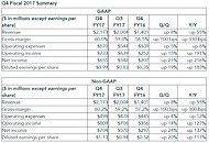
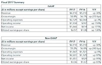
For fiscal 2017, revenue reached a record $6.91 billion, up 38 percent from $5.01 billion a year earlier. GAAP earnings per diluted share were $2.57, up 138 percent from $1.08 a year earlier. Non-GAAP earnings per diluted share were $3.06, up 83 percent from $1.67 a year earlier. "We had a great finish to a record year, with continued strong growth across all our businesses," said Jen-Hsun Huang, founder and chief executive officer of NVIDIA. "Our GPU computing platform is enjoying rapid adoption in artificial intelligence, cloud computing, gaming, and autonomous vehicles.‎

NVIDIA Unveils New Line of Quadro Pascal GPUs

NVIDIA today introduced a range of Quadro products, all based on its Pascal architecture, that transform desktop workstations into supercomputers with breakthrough capabilities for professional workflows across many industries. Workflows in design, engineering and other areas are evolving rapidly to meet the exponential growth in data size and complexity that comes with photorealism, virtual reality and deep learning technologies. To tap into these opportunities, the new NVIDIA Quadro Pascal-based lineup provides an enterprise-grade visual computing platform that streamlines design and simulation workflows with up to twice the performance of the previous generation, and ultra-fast memory.

"Professional workflows are now infused with artificial intelligence, virtual reality and photorealism, creating new challenges for our most demanding users," said Bob Pette, vice president of Professional Visualization at NVIDIA. "Our new Quadro lineup provides the graphics and compute performance required to address these challenges. And, by unifying compute and design, the Quadro GP100 transforms the average desktop workstation with the power of a supercomputer."

NVIDIA Tesla P100 Available on Google Cloud Platform

NVIDIA announced that its flagship GPGPU accelerator, the Tesla P100, will be available through Google Cloud Platform. The company's Tesla K80 accelerator will also be offered. The Google Cloud Platform allows customers to perform specific computing tasks at an infinitesimally lower cost than having to rent hardware in-situ or having to buy it; by offloading your computing tasks to offsite data-centers. IT professionals can build and deploy servers, HPC farms, or even supercomputers, of all shapes and sizes within hours of placing an order online with Google.

The Tesla P100 is a GPGPU with the most powerful GPU in existence - the NVIDIA GP100 "Pascal," featuring 3,584 CUDA cores, up to 16 GB of HBM2 memory, and NVLink high-bandwidth interconnect support. The other high-end GPU accelerators on offer by Google are the Tesla K80, based on a pair of GK210 "Kepler" GPUs, and the AMD FirePro S9300 X2, based on a pair of "Fiji" GPUs.

NVIDIA to Unveil GeForce GTX TITAN P at Gamescom

NVIDIA is preparing to launch its flagship graphics card based on the "Pascal" architecture, the so-called GeForce GTX TITAN P, at the 2016 Gamescom, held in Cologne, Germany, between 17-21 August. The card is expected to be based on the GP100 silicon, and could likely come in two variants - 16 GB and 12 GB. The two differ by memory bus width besides memory size. The 16 GB variant could feature four HBM2 stacks over a 4096-bit memory bus; while the 12 GB variant could feature three HBM2 stacks, and a 3072-bit bus. This approach by NVIDIA is identical to the way it carved out Tesla P100-based PCIe accelerators, based on this ASIC. The cards' TDP could be rated between 300-375W, drawing power from two 8-pin PCIe power connectors.

The GP100 and GTX TITAN P isn't the only high-end graphics card lineup targeted at gamers and PC enthusiasts, NVIDIA is also working the GP102 silicon, positioned between the GP104 and the GP100. This chip could lack FP64 CUDA cores found on the GP100 silicon, and feature up to 3,840 CUDA cores of the same kind found on the GP104. The GP102 is also expected to feature simpler 384-bit GDDR5X memory. NVIDIA could base the GTX 1080 Ti on this chip.

NVIDIA Announces a PCI-Express Variant of its Tesla P100 HPC Accelerator

NVIDIA announced a PCI-Express add-on card variant of its Tesla P100 HPC accelerator, at the 2016 International Supercomputing Conference, held in Frankfurt, Germany. The card is about 30 cm long, 2-slot thick, and of standard height, and is designed for PCIe multi-slot servers. The company had introduced the Tesla P100 earlier this year in April, with a dense mezzanine form-factor variant for servers with NVLink.

The PCIe variant of the P100 offers slightly lower performance than the NVLink variant, because of lower clock speeds, although the core-configuration of the GP100 silicon remains unchanged. It offers FP64 (double-precision floating-point) performance of 4.70 TFLOP/s, FP32 (single-precision) performance of 9.30 TFLOP/s, and FP16 performance of 18.7 TFLOP/s, compared to the NVLink variant's 5.3 TFLOP/s, 10.6 TFLOP/s, and 21 TFLOP/s, respectively. The card comes in two sub-variants based on memory, there's a 16 GB variant with 720 GB/s memory bandwidth and 4 MB L3 cache, and a 12 GB variant with 548 GB/s and 3 MB L3 cache. Both sub-variants feature 3,584 CUDA cores based on the "Pascal" architecture, and core clock speed of 1300 MHz.

NVIDIA GeForce GTX 1080 Ti to be Based on GP102 Silicon

It looks like NVIDIA will have not one, but two "big chips" based on the "Pascal" architecture. The first one of course is the GP100, which made its debut with the Tesla P100 HPC processor. The GP100 is an expensive chip at the outset, featuring a combination of FP32 (single-precision) and FP64 (double-precision) CUDA cores, running up to 3,840 SPFP and 1,920 DPFP, working out to a gargantuan 5,760 CUDA core count. FP64 CUDA cores are practically useless on the consumer-graphics space, particularly in the hands of gamers. The GP100 also features a swanky 4096-bit HBM2 memory interface, with stacked memory dies sitting on the GPU package, making up an expensive multi-chip module. NVIDIA also doesn't want its product development cycle to be held hostage by HBM2 market availability and yields.

NVIDIA hence thinks there's room for a middle-ground between the super-complex GP100, and the rather simple GP104, if a price-war with AMD should make it impossible to sell a GP100-based SKU at $650-ish. Enter the GP102. This ASIC will be targeted at consumer graphics, making up GeForce GTX products, including the GTX 1080 Ti. It is cost-effective, in that it does away with the FP64 CUDA cores found on the GP100, retaining just a 3,840 FP32 CUDA cores count, 33% higher than that of the GP104, just as the GM200 had 33% more CUDA cores than the GM204.

NVIDIA to Launch Mid-range GP106 Based Graphics Cards in Autumn 2016

NVIDIA is expected to launch the first consumer graphics cards based on the GP106 silicon some time in Autumn 2016 (late Q3-early Q4). Based on the company's next-generation "Pascal" architecture, the GP106 will drive several key mid-range and performance-segment (price/performance sweetspot) SKUs, including the cards that succeed the current GeForce GTX 960 and GTX 950. Based on the way NVIDIA's big GP100 silicon is structured, assuming the GP106 features two graphics processing clusters (GPCs), the way the current GM206 silicon does; one can expect a CUDA core count in the neighborhood of 1,280. NVIDIA could use this chip to capture several key sub-$250 price points.

NVIDIA "Pascal" GP100 Silicon Detailed

The upcoming "Pascal" GPU architecture from NVIDIA is shaping up to be a pixel-crunching monstrosity. Introduced as more of a number-cruncher in its Tesla P100 unveil at GTC 2016, we got our hands on the block diagram of the "GP100" silicon which drives it. To begin with, the GP100 is a multi-chip module, much like AMD's "Fiji," consisting of a large GPU die, four memory-stacks, and silicon wafer (interposer) acting as substrate for the GPU and memory stacks, letting NVIDIA drive microscopic wires between the two. The GP100 features a 4096-bit wide HBM2 memory interface, with typical memory bandwidths of up to 1 TB/s. On the P100, the memory ticks at 720 GB/s.

At its most top-level hierarchy, the GP100 is structured much like other NVIDIA GPUs, with the exception of two key interfaces - bus and memory. A PCI-Express gen 3.0 x16 host interface connects the GPU to your system, the GigaThread Engine distributes workload between six graphics processing clusters (GPCs). Eight memory controllers make up the 4096-bit wide HBM2 memory interface, and a new "High-speed Hub" component, wires out four NVLink ports. At this point it's not known if each port has a throughput of 80 GB/s (per-direction), or all four ports put together.

NVIDIA's Next Flagship Graphics Cards will be the GeForce X80 Series

With the GeForce GTX 900 series, NVIDIA has exhausted its GeForce GTX nomenclature, according to a sensational scoop from the rumor mill. Instead of going with the GTX 1000 series that has one digit too many, the company is turning the page on the GeForce GTX brand altogether. The company's next-generation high-end graphics card series will be the GeForce X80 series. Based on the performance-segment "GP104" and high-end "GP100" chips, the GeForce X80 series will consist of the performance-segment GeForce X80, the high-end GeForce X80 Ti, and the enthusiast-segment GeForce X80 TITAN.

Based on the "Pascal" architecture, the GP104 silicon is expected to feature as many as 4,096 CUDA cores. It will also feature 256 TMUs, 128 ROPs, and a GDDR5X memory interface, with 384 GB/s memory bandwidth. 6 GB could be the standard memory amount. Its texture- and pixel-fillrates are rated to be 33% higher than those of the GM200-based GeForce GTX TITAN X. The GP104 chip will be built on the 16 nm FinFET process. The TDP of this chip is rated at 175W.

NVIDIA to Unveil "Pascal" at the 2016 Computex

NVIDIA is reportedly planning to unveil its next-generation GeForce GTX "Pascal" GPUs at the 2016 Computex show, in Taipei, scheduled for early-June. This unveiling doesn't necessarily mean market availability. SweClockers reports that problems, particularly related to NVIDIA supplier TSMC getting its 16 nm FinFET node up to speed, especially following the recent Taiwan earthquake, could delay market available to late- or even post-Summer. It remains to be seen if the "Pascal" architecture debuts as an all-mighty "GP100" chip, or a smaller, performance-segment "GP104" that will be peddled as enthusiast-segment over being faster than the current big-chip, the GM200. NVIDIA's next generation GeForce nomenclature will also be particularly interesting to look out for, given that the current lineup is already at the GTX 900 series.

NVIDIA GP100 Silicon to Feature 4 TFLOPs DPFP Performance

NVIDIA's upcoming flagship GPU based on its next-generation "Pascal" architecture, codenamed GP100, is shaping up to be a number-crunching monster. According to a leaked slide by an NVIDIA research fellow, the company is designing the chip to serve up double-precision floating-point (DPFP) performance as high as 4 TFLOP/s, a 3-fold increase from the 1.31 TFLOP/s offered by the Tesla K20, based on the "Kepler" GK110 silicon.

The same slide also reveals single-precision floating-point (SPFP) performance to be as high as 12 TFLOP/s, four times that of the GK110, and nearly double that of the GM200. The slide also appears to settle the speculation on whether GP100 will use stacked HBM2 memory, or GDDR5X. Given the 1 TB/s memory bandwidth mentioned on the slide, we're inclined to hand it to stacked HBM2.

NVIDIA GP100 Silicon Moves to Testing Phase

NVIDIA's next-generation flagship graphics processor, codenamed "GP100," has reportedly graduated to testing phase. That is when a limited batch of completed chips are sent from the foundry partner to NVIDIA for testing and evaluation. The chips tripped speed-traps on changeover airports, on their way to NVIDIA. 3DCenter.org predicts that the GP100, based on the company's "Pascal" GPU architecture, will feature no less than 17 billion transistors, and will be built on the 16 nm FinFET+ node at TSMC. The GP100 will feature an HBM2 memory interface. HBM2 allows you to cram up to 32 GB of memory. The flagship product based on GP100 could feature about 16 GB of memory. NVIDIA's design goal could be to squeeze out anywhere between 60-90% higher performance than the current-generation flagship GTX TITAN-X.

NVIDIA Tapes Out "Pascal" Based GP100 Silicon

Sources tell 3DCenter.org that NVIDIA has successfully taped out its next big silicon based on its upcoming "Pascal" GPU architecture, codenamed GP100. A successor to GM200, this chip will be the precursor to several others based on this architecture. A tape-out means that the company has successfully made a tiny quantity of working prototypes for internal testing and further development. It's usually seen as a major milestone in a product development cycle.

With "Pascal," NVIDIA will pole-vault HBM1, which is making its debut with AMD's "Fiji" silicon; and jump straight to HBM2, which will allow SKU designers to cram up to 32 GB of video memory. 3DCenter.org speculates that GP100 could feature anywhere between 4,500 to 6,000 CUDA cores. The chip will be built on TSMC's upcoming 16 nanometer silicon fab process, which will finally hit the road by 2016. The GP100, and its companion performance-segment silicon, the GP104 (successor to GM204), are expected to launch between Q2 and Q3, 2016.
Return to Keyword Browsing
Apr 29th, 2024 21:25 EDT change timezone

New Forum Posts

Popular Reviews

Controversial News Posts